Loading driving device

a technology of driving device and load, which is applied in the direction of printed circuit board receptacles, electrical apparatus construction details, support structure mounting, etc., to achieve the effect of reducing the mounting area of the output power device and the driving ic, and high speed

Inactive Publication Date: 2008-01-10
DENSO CORP
View PDF14 Cites 19 Cited by
  • Summary
  • Abstract
  • Description
  • Claims
  • Application Information

AI Technical Summary

Benefits of technology

[0012] In the above device, since the wire between the output power device and the driving IC is short, the output power device is controlled with high speed. Further, a mounting area of the output power device and the driving IC is reduced.

Problems solved by technology

However, there is no disclosure in JP-A-2005-175130 that the driving IC is also mounted on the same electrode plate.

Method used


Image

  • Loading driving device
  • Loading driving device
  • Loading driving device

Examples


first embodiment

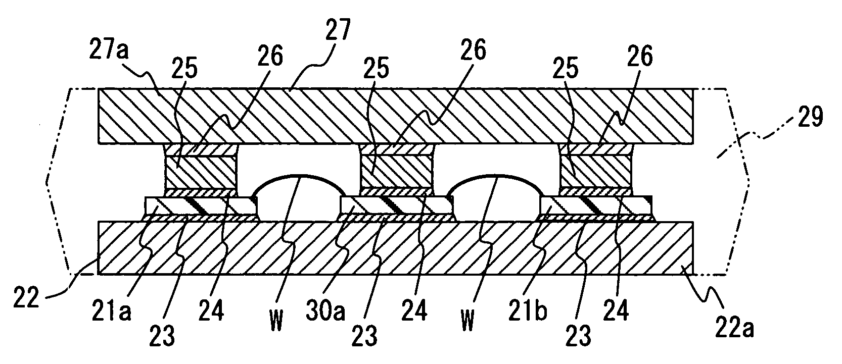
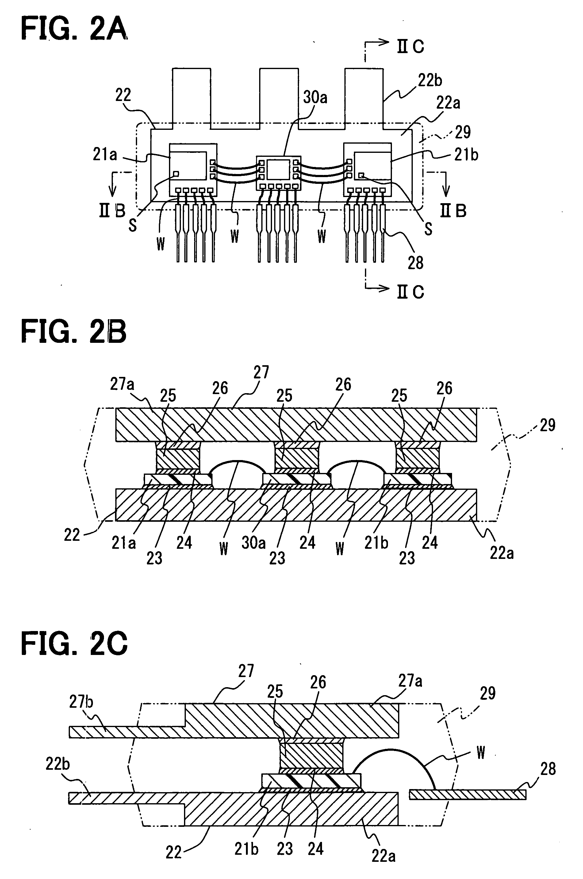
[0029] A load driving device is suitably used for an inverter system of a EHV (i.e., electric and hybrid vehicle). FIG. 1 shows the inverter system, and FIGS. 2A-2C show a semiconductor module. FIG. 3 shows a power device such as an IGBT, and FIGS. 4A-4C show a HVIC (i.e., high voltage IC).

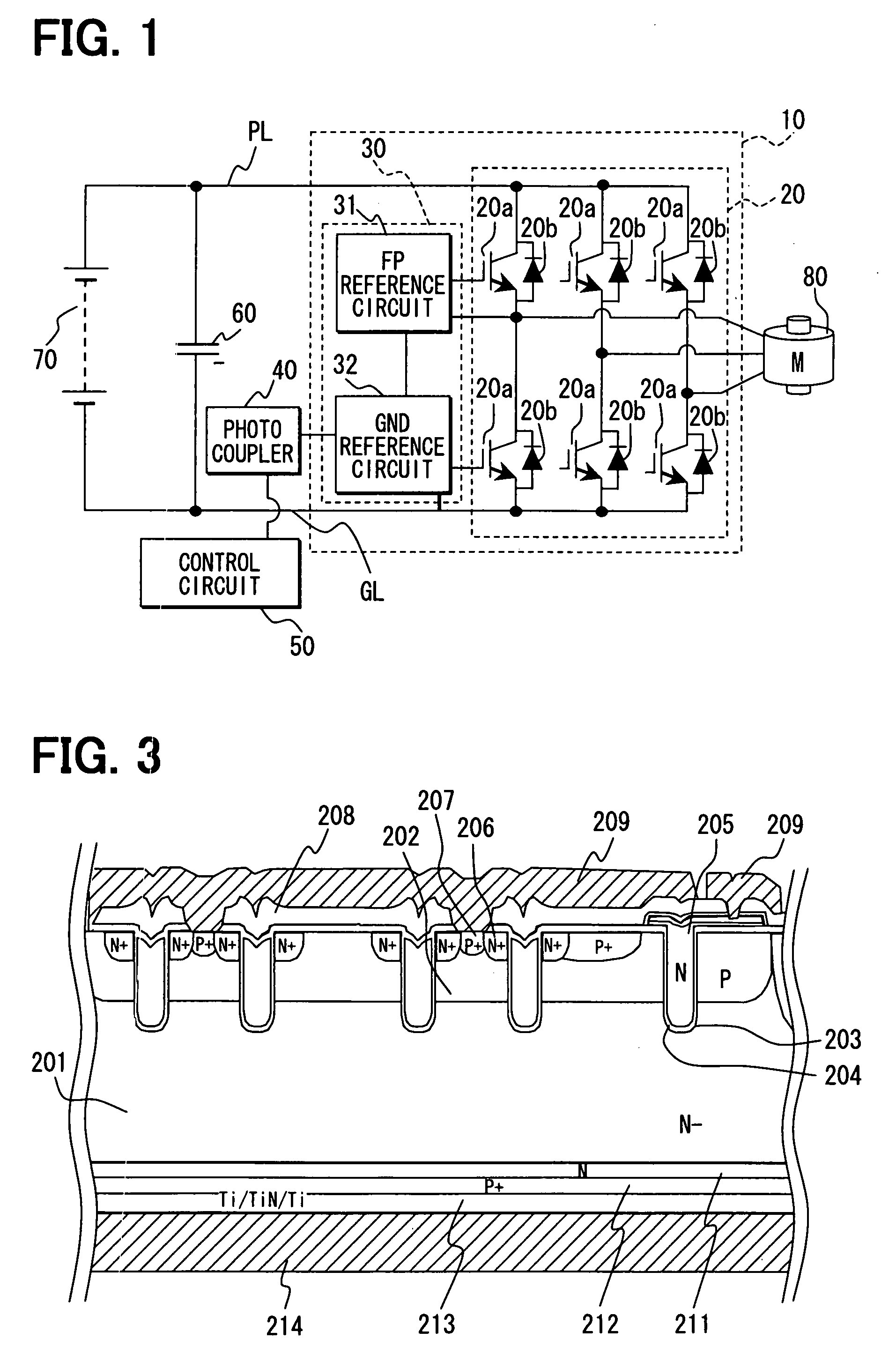
[0030] In FIG. 1, the inverter system includes the semiconductor module 10, a photo coupler 40, a control circuit 50, a capacitor 60, a main battery 70 and a motor 80. The semiconductor module 10 is an inverter having a power device portion 20 and a driving IC portion 30. Here, PL represents a power source line, and GL represents a ground line.

[0031] The main battery 70 is a direct current power source, and formed from a secondary battery such as a lithium-ion secondary battery and a nickel hydrogen battery. The main battery 70 supplies a direct current to the inverter such as the semiconductor module 10. The capacitor 60 is a smoothing capacitor, and connected between the power source line PL a...

second embodiment

[0061]FIGS. 7A and 7B show a semiconductor module, and FIG. 8 shows another semiconductor module, according to a second embodiment.

[0062] The above semiconductor modules have difference from the module shown in FIG. 1, which is a mounting position of the HVIC 30a in the semiconductor module.

[0063] In FIG. 7A, the power devices 21a, 21b and the diode 20b are electrically connected to the electrode plate 22 with the wire W, and the power devices 21a, 21b and the diode 20b are mounted on the plate 22 with a connection member (not shown) made of conductive material such as solder so that they are electrically connected to the plate 22. As shown in FIG. 7B, the HVIC 30a is formed on the power device 21a with the connection member 24. Thus, the power device 21a and the HVIC 30a are electrically connected to each other. The spacer element 25 is electrically connected to and mounted on the HVIC 30a with the connection member 24. The spacer element 25 is electrically connected to the elect...

third embodiment

[0067]FIGS. 9A and 9B show a semiconductor module, FIG. 10 shows another semiconductor module, and FIG. 11 shows further another semiconductor module, according to a third embodiment.

[0068] The above semiconductor modules have difference from the module shown in FIG. 1, which is an electrode plate.

[0069] As shown in FIG. 9B, the power devices 21a, 21b and the HVIC 30a are mounted on the electrode plate 22 through the connection member 23, and electrically connected to the electrode plate 22 with the wire W. The power devices 21a, 21b are electrically connected to the spacer element 25 with the connection member 24. Specifically, the spacer element 25 is bonded to one side of the power devices 21a, 21b, the one side which is opposite to the electrode plate 22. Further, the spacer element 25 is connected to the heat radiation plate 271 with the connection member 26. The heat radiation plate 271 is made of, for example, copper, and has an opening corresponding to the HVIC 30a. Thus, ...


PUM


Abstract

A load driving device includes: an output power device for driving a load; a driving IC for controlling the output power device, wherein the driving IC is electrically coupled with the output power device through a wire or a connection member; and a first electrode substrate. The output power device and the driving IC are mounted on the first electrode substrate. In this case, the output power device is controlled with high speed, and a mounting area of the output power device and the driving IC is reduced.

Description

CROSS REFERENCE TO RELATED APPLICATIONS [0001] This application is based on Japanese Patent Applications No. 2006-156686 filed on Jun. 5, 2006, and No. 2007-116133 filed on Apr. 25, 2007, the disclosures of which are incorporated herein by reference. FIELD OF THE INVENTION [0002] The present invention relates to a load driving device. BACKGROUND OF THE INVENTION [0003] A load driving device is shown in, for example, JP-A-2005-175130. The device includes an inverter, a signal generator and a control circuit. The signal generator receives a signal from the control circuit and generates a PWM (i.e., pulse width modulation) signal, which provides to turn on and off an output power device of the inverter. The inverter includes the output power device such as an IGBT, a driving IC for receiving the PWM signal from the signal generator and for operating to switch on and off the output power device, and a reverse parallel connection diode for flowing current from an emitter to a collector i...

Claims


Application Information

Patent Timeline
Patent Type & Authority Applications(United States)
IPC IPC(8): H02M7/537H05K7/20
CPCH01L2224/32245H01L2924/1301H01L2224/48247H01L2224/73265H01L2924/01046H02M7/003H05K7/1432H01L2224/48091H01L2924/13091H01L2224/73215H01L2224/33181H01L2224/32145H01L2924/13055H01L2224/48137H01L2924/1305H01L2924/00014H01L2924/00H01L2924/00012H01L24/73H01L2924/14H01L2924/181H01L2224/2612H05K7/14329
Inventor SHIRAKI, SATOSHIYAMADA, AKIRABAN, HIROYUKI
Owner DENSO CORP
Why Eureka
Try Eureka