Semiconductor package and method of making the same

a semiconductor and package technology, applied in the manufacture of printed circuits, printed circuit aspects, basic electric elements, etc., can solve the problems of wasting a lot of fabrication materials, affecting the overall thickness and size of the circuit board, and affecting the quality of the product, so as to reduce the overall size of the semiconductor package, avoid problems, and save production materials

Inactive Publication Date: 2008-01-10
SILICONWARE PRECISION IND CO LTD
View PDF6 Cites 10 Cited by
  • Summary
  • Abstract
  • Description
  • Claims
  • Application Information

AI Technical Summary

Benefits of technology

[0027] Accordingly, unlike the prior arts, the present invention does not need to form any electrical terminal of 0.38 mm in thickness on the circuit board, thereby avoiding forming any circuit board that cannot match with the specification for circuit board in the industry or cannot be implemented in practice. Moreover, since there is no need of forming an additional electrical terminal that has a thickness of 0.38 mm, the thickness of the circuit board can therefore become lighter, thinner, shorter, and smaller, thereby minimizing the overall size of a semiconductor package and avoiding problems such as wasting production material and increasing fabrication cost and time.
[0028] Last but not the least, the lead frame mounted on the circuit board can be employed to dissipate heat more effectively for electronic devices, so as to enhance product reliability.

Problems solved by technology

However, in practical implementations, forming an electrical terminal of 0.38 mm in thickness (i.e. 380 μm) on the circuit board is beyond the current industry standard for circuit boards and the industry's ability to fabricating the same.
Therefore, if an electrical terminal of a circuit board is fabricated to have a thickness of about 380 μm in accordance with the requirements of USB Association, the overall thickness and size of the circuit board may be dramatically increased to an undesired level, and the fabrication processes may be extremely difficult to implement.
Moreover, if such massive structure is to be applied to a semiconductor package, not only that the package can never become lighter, thinner, shorter, and smaller, but bulkier, configuration as such also wastes a lot of fabrication materials, thereby increasing fabrication time and cost.
Solutions to these problems have been long sought but prior developments have not taught or suggested any solutions and, thus, solutions to these problems have long eluded those skilled in the art.

Method used


Image

  • Semiconductor package and method of making the same
  • Semiconductor package and method of making the same
  • Semiconductor package and method of making the same

Examples


first embodiment

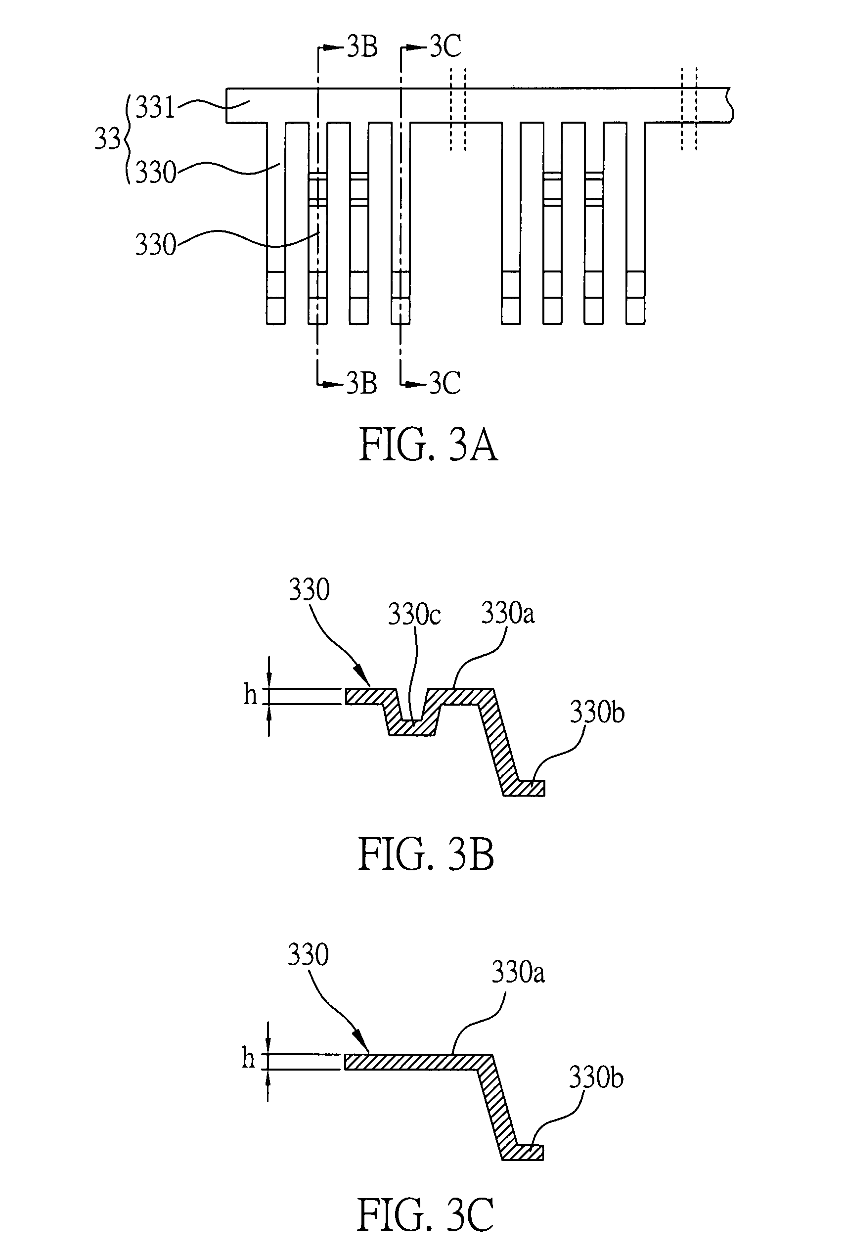
[0039]FIGS. 3A to 3I are schematic views showing a semiconductor package and method of fabricating the same according to a first embodiment of the present invention. In this preferred embodiment, the fabrication method of the present invention is applied to single production, however it is also applicable to batch production for enhancing production efficiency and yield.

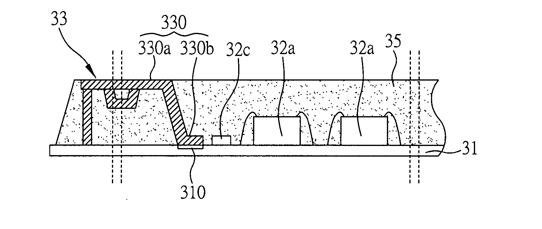
[0040] First, as shown in FIGS. 3A to 3C, a modular structure having a plurality of lead frames 33 is provided, wherein each of the lead frames 33 has a plurality of terminal leads 330 configured horizontally. Furthermore, the terminal leads 330 are connected to each other by a guiding guiding rail 331, wherein each of the terminal leads 330 further comprises a flat portion 330a and a contacting portion 330b downwardly bent from an edge of the flat portion 330a. FIGS. 3B and 3C in conjunction with FIG. 3A depict cross-sectional views of different kinds of terminal leads 330 of the lead frame 33.

[0041] One of the fe...

second embodiment

[0050]FIGS. 4A to 4G are schematic views showing a semiconductor package and method of fabricating the same according to a second embodiment of the present invention.

[0051] First, as shown in FIGS. 4A to 4C, a lead frame 43 is provided. The lead frame 43 comprises a plain portion 43a, at least a contacting portion 43b formed on and extending downwardly from at least a side of the plain portion 43a, and a plurality of terminal leads 430, wherein the terminal leads 430 are formed on at least a side of the lead frame 43 and separated from each other horizontally. Furthermore, each of the terminal leads 430 is configured to have a flat portion 43a′ and a contacting portion 43b′ extending downwardly from the flat portion 43a′. FIGS. 4B and 4C in conjunction with FIG. 4A depict cross-sectional views of different kinds of terminal leads 430.

[0052] In order to allow the terminal leads 430 to act as electrical terminals of an USB memory card, the thickness h of each of the terminal leads 4...

third embodiment

[0059]FIGS. 5A to 5I are schematic views showing a semiconductor package and method of fabricating the same according to a third embodiment of the present invention, wherein the third embodiment is a more preferable embodiment of the present invention.

[0060] As shown in FIGS. 5A and 5B, a lead frame 53 is provided, wherein FIG. 5B is a cross-sectional view of the lead frame 53 corresponding to FIG. 5A. The lead frame 53 comprises a plain portion 53a, at least a contacting portion 53b formed on and extending downwardly from at least a side of the plain portion 53a, and a plurality of terminal leads 530, wherein the terminal leads 530 are formed on at least a side of the lead frame 53 and separated from each other horizontally. Furthermore, each of the terminal leads 530 is configured to have a flat portion 53a′ and a contacting portion 53b′ extending downwardly from the flat portion 53a′.

[0061] Furthermore, in order to satisfy and conform with the requirements and standards of USB ...


PUM


Abstract

A semiconductor package and its fabrication method are disclosed. The fabrication method has the steps of: providing at least a lead frame having a plurality of terminal leads formed with flat portions and contacting portions, providing at least a circuit board having a plurality of electrical connection pads, mounting the contacting portions on and electrically connecting to the electrical connection pads, attaching and electrically connecting electronic elements to the circuit board, forming an encapsulant for encapsulating the lead frames and the electronic elements but uncovering the flat portions of the terminal leads, and cutting around the circuit board along a cutting path that crosses through each of the terminal leads so as to allow each of the terminal leads to be electrically independent, wherein the terminal leads are employed to act as the electrical terminals of USB memory cards for storing or retrieving data.

Description

FIELD OF THE INVENTION [0001] The present invention is related to semiconductor packages and methods of making the same, and more particularly, to a semiconductor package and a method of making the same, which are applicable to universal serial bus (USB) memory cards. BACKGROUND OF THE INVENTION [0002] Referring to FIG. 1, a prior-art universal serial bus (USB) memory card comprises a circuit board 11, a flash integrated circuit (IC) 12a, a controller IC 12b, and passive components 12c, wherein the flash IC 12a, the controller IC 12b, and the passive components 12c are mounted on and electrically connect to the circuit board 11 first, and then an USB plug 13 is soldered on the circuit board 11 before using a casing 14 to enclose the foregoing components to form the USB memory card. Similar techniques may be found in U.S. Pat. Nos. 6,854,984 and 6,813,164. [0003] Nevertheless, because the size of the aforementioned USB plug is too big to be applied to any lighter, thinner, shorter, a...

Claims


Application Information

Patent Timeline
Patent Type & Authority Applications(United States)
IPC IPC(8): H01R12/04H01L23/04
CPCH01L23/4334H01L23/49855H01L2924/16152H01L2924/1815H01L2224/48227H05K3/284H05K2201/10159H05K2201/1034H05K2201/10924H05K1/117
Inventor TAN, TONIADYYU, CHENG-CHUNGWEI, HUNG-CHICHANG, CHIH-HOULI, HUAN-SHIANG
Owner SILICONWARE PRECISION IND CO LTD
Why Eureka
Try Eureka