Semiconductor device verification system and semiconductor device fabrication method

Inactive Publication Date: 2008-01-10
SOCIONEXT INC
View PDF1 Cites 15 Cited by
  • Summary
  • Abstract
  • Description
  • Claims
  • Application Information

AI Technical Summary

Benefits of technology

[0020]The integration level of LSI is rising. Such LSI

Problems solved by technology

However, there is a limit to design made by hand because of such a rise in the integration level of LSI.
However, the physical verification system which performs a process by skipping the data included in the excluded cell list of the layout data has the following problems.
Therefore, if interference such as a wiring from the outside exists at a tier higher than the excluded cell, the interference cannot be detected.
Accordingly, each cell of the layout always suffers interference of some kind.
However, if an interference prohibition area is set, the area of the layout increases, complexity increases because of, for example, a need to consider the achievement of a balance between the interference prohibition area and an interference permissible area, and the possibility of an increase in processing time and a deterioration in verification accuracy increases.
However, interference may occur between data corresponding to a tier higher than

Method used


Image

  • Semiconductor device verification system and semiconductor device fabrication method
  • Semiconductor device verification system and semiconductor device fabrication method
  • Semiconductor device verification system and semiconductor device fabrication method

Examples


Embodiment Construction

[0043]An embodiment of the present invention will now be described in detail with reference to the drawings.

[0044]An overview of the present invention will be described first.

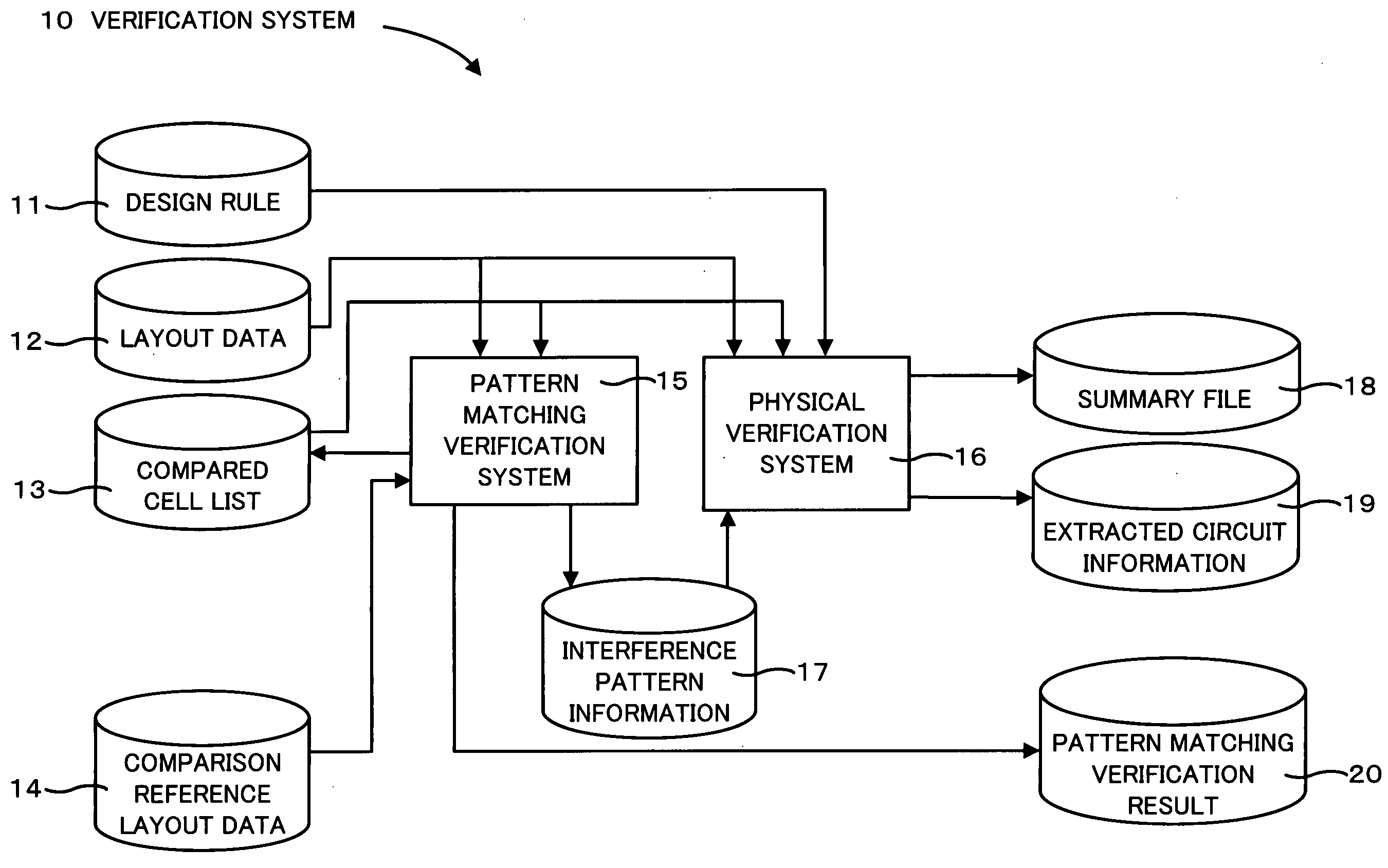
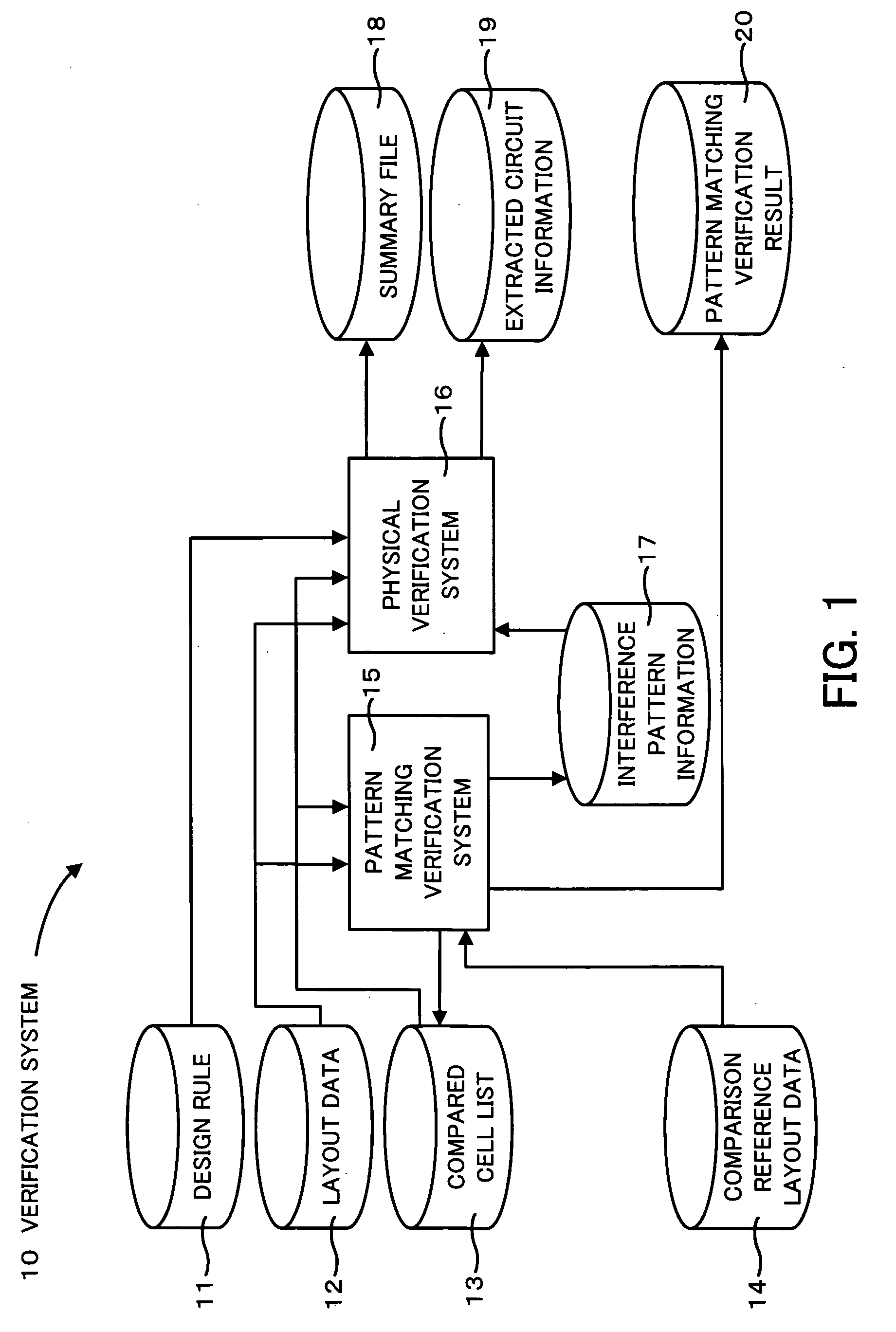
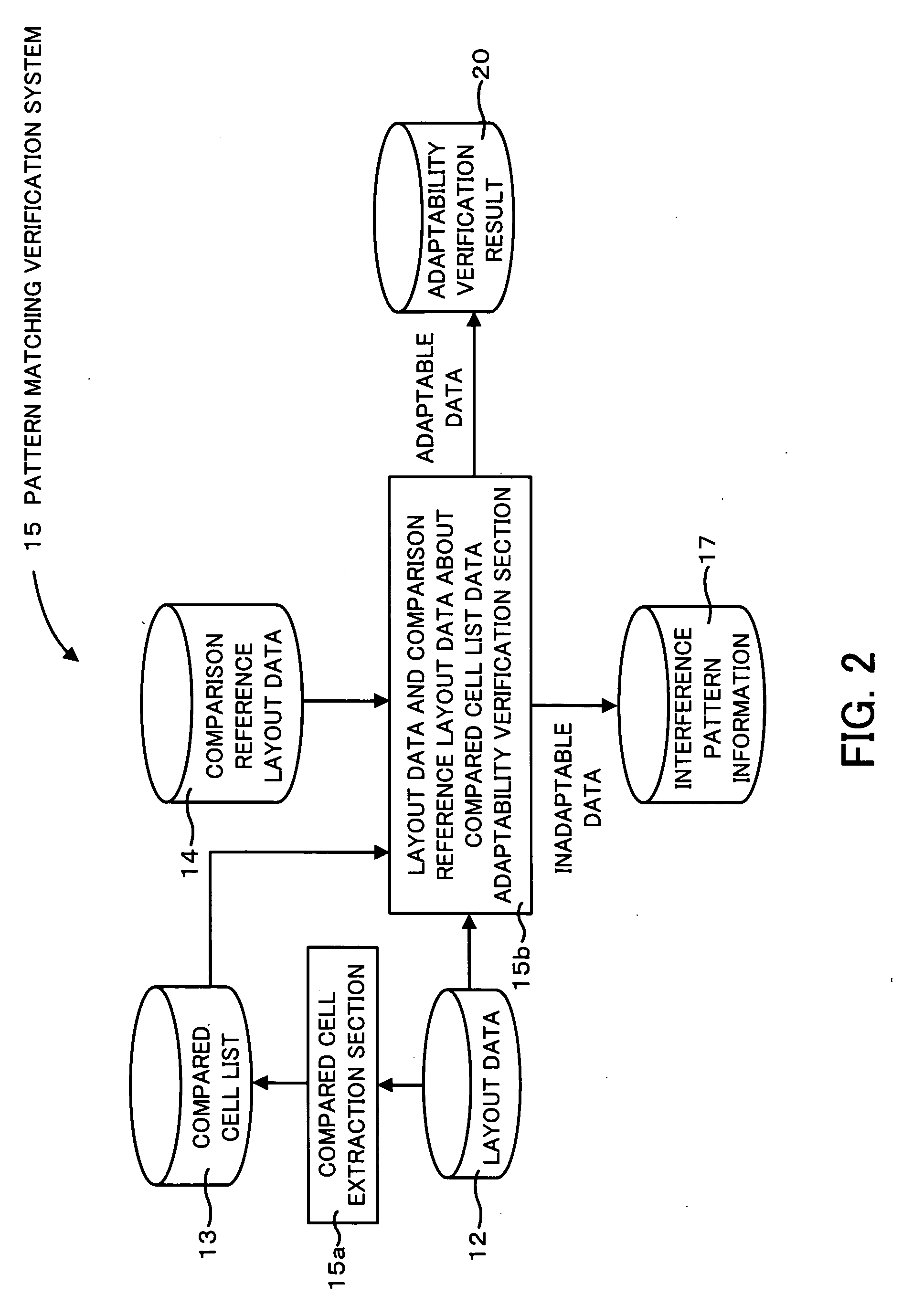
[0045]FIG. 1 is a schematic view showing a verification system according to the present invention. FIG. 2 is a schematic view showing a pattern matching verification system. FIG. 3 is a schematic view showing a physical verification system. FIG. 4 is a schematic view showing a semiconductor integrated circuit designed on the basis of layout data.

[0046]FIGS. 5 through 7 are schematic views showing an embodiment of the present invention.

[0047]As shown in FIG. 1, a verification system 10 according to the present invention comprises a pattern matching verification system 15 and a physical verification system 16 in order to verify layout data 12 generated by layout design. The pattern matching verification system 15 extracts interference pattern information 17. The physical verification system 16 also verifies the i...


PUM


Abstract

A semiconductor device verification system capable of verifying operation with great accuracy. A pattern matching verification system outputs interference pattern information. A physical verification system compiles the interference pattern information and a design rule and extracts a design rule applied to the interference pattern information. The physical verification system then refers to the design rule to verify a compared cell list and the interference pattern information. As a result, the physical verification system can perform physical verification of layout data without skipping data regarding the compared cell list.

Description

CROSS-REFERENCE TO RELATED APPLICATIONS[0001]This application is based upon and claims the benefits of priority from the prior Japanese Patent Application No. 2006-184722, filed on Jul. 4, 2006, the entire contents of which are incorporated herein by reference.BACKGROUND OF THE INVENTION[0002](1) Field of the Invention[0003]This invention relates to a semiconductor device verification system and a semiconductor device fabrication method and, more particularly, to a semiconductor device verification system for verifying layout data generated by the layout design of a semiconductor device and a semiconductor device fabrication method.[0004](2) Description of the Related Art[0005]For example, the number of transistors included in large-scale integration (LSI) was about a thousand at first. With the progress of semiconductor technology, however, ten million to several hundred million transistors can be formed in LSI at present.[0006]In addition, LSI design was made mainly by hand at fir...

Claims


Application Information

Patent Timeline
IPC IPC(8): G06F17/50
CPCG06F17/5081G06F30/398
Inventor KOIZUMI, RYOJI
Owner SOCIONEXT INC
Why Eureka
Try Eureka