Semiconductor device having pads for bonding and probing
- Summary
- Abstract
- Description
- Claims
- Application Information
AI Technical Summary
Benefits of technology
Problems solved by technology
Method used
Image
Examples
first embodiment
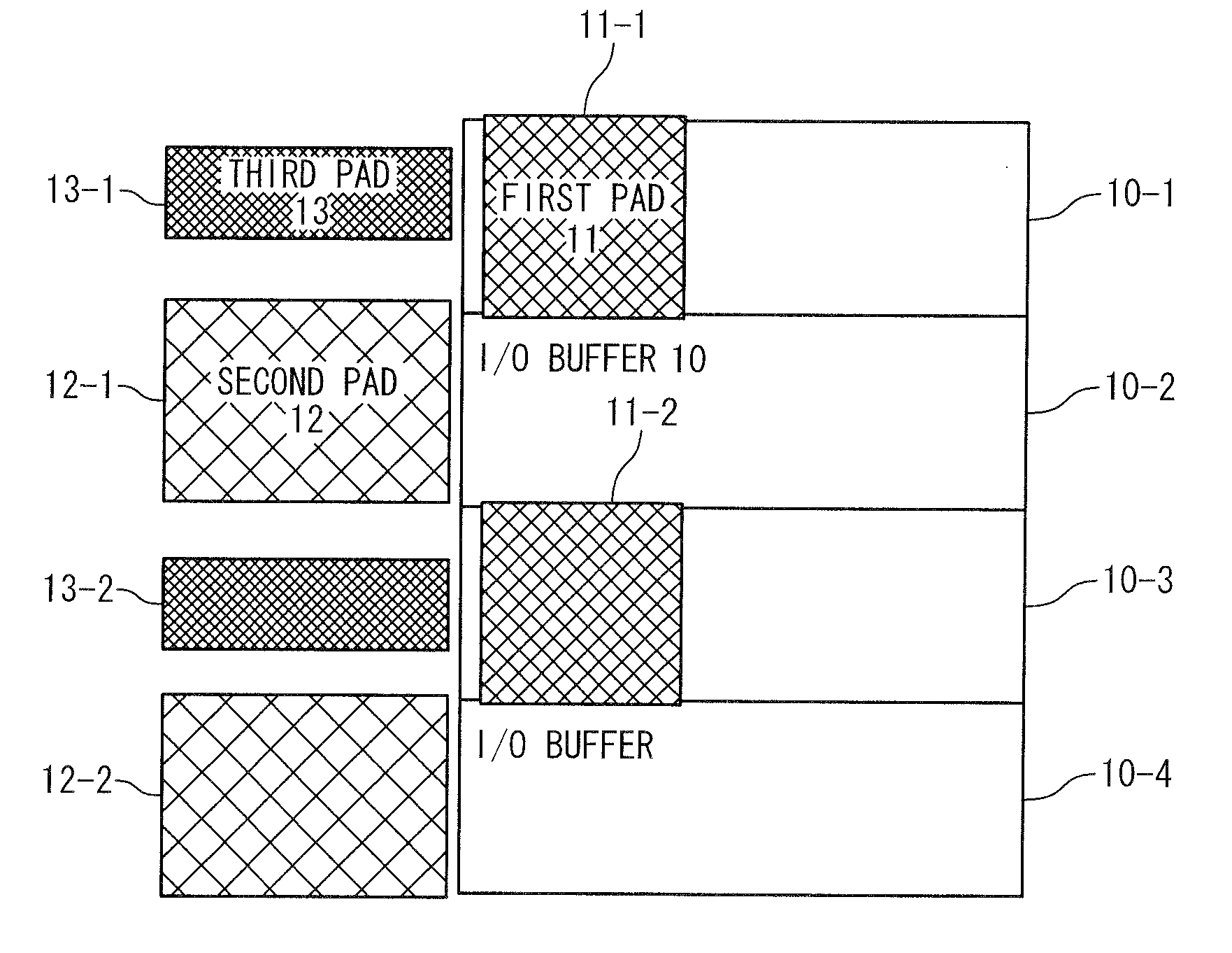
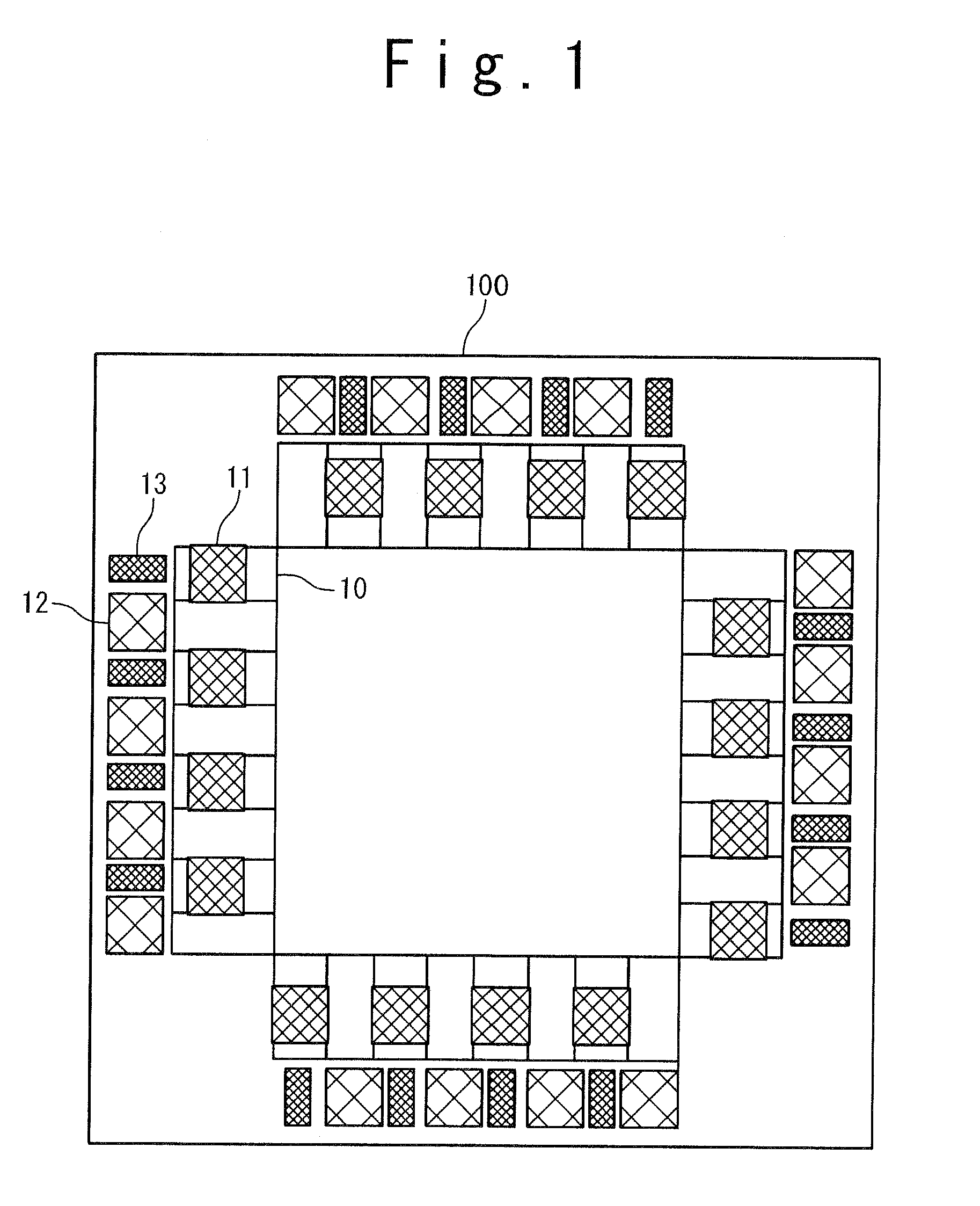
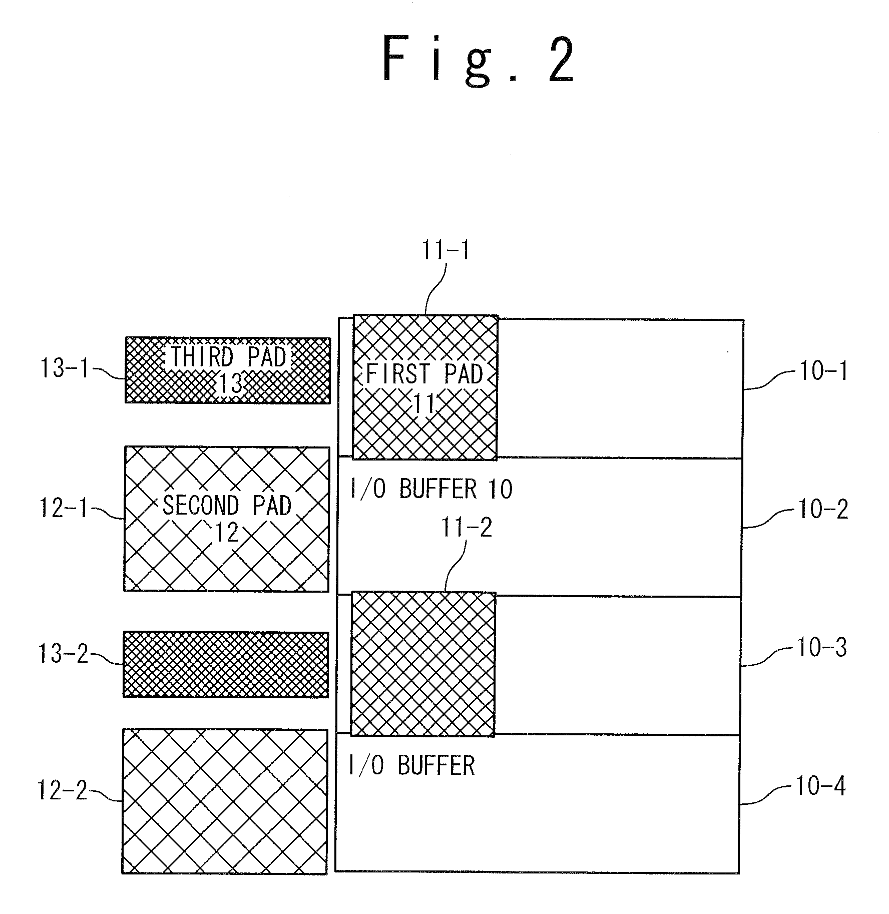
[0036]Referring not to FIG. 1, a semiconductor device according to the present invention includes an I / O buffer 10, a first pad 11, a second pad 12, and a third pad 13.
[0037]The semiconductor device 100 of this embodiment is provided with a rectangular semiconductor chip in which internal interconnection layers having a laminated structure of a plurality of layers and internal elements are formed, and includes various kinds of processing circuit inside, and includes the I / O buffer 10 on respective sides of circumference part. In addition, the first pad 11 is formed on an uppermost part in an area where the I / O buffer is formed. The second pad 12 and the third pad 13 are further formed outside the above-described area.
[0038]In FIG. 2, only a part of one side of the semiconductor device is shown to describe the first, second, and third pads for simplification.
[0039]Each I / O buffer 10-i (i=1 to n: n is an arbitrary natural number) of the I / O buffers 10 represents an inputting and outpu...
second embodiment
[0066]Referring to FIGS. 5A, 5B, and 5C, the present invention will be explained below.
[0067]The present embodiment contributes to a reduction of a chip size by arranging first pads 11, second pads 12 and third pads 13 on an I / O buffer 10 so that an area where only pads are formed on is reduced. A structure formed under the second pads and the third pads is durable against the impact of probing applied to the pads. That is to say, the structure includes a stress relaxation layer (stress absorbing layer). As an example of the stress absorbing layer, a layer on which no element or circuit is formed is provided just under the pad layer. Or the stress absorbing layer is an interconnection layer which is not used as a part of an electrical circuit of the semiconductor chip. Or structural material provided to form a metal layer does not exist in the stress absorbing layer. As another example of the stress absorbing layer, the stress absorbing layer can be constructed by a thick interlayer...
third embodiment
[0078]Referring to FIGS. 6, 7, and 8, the present invention will be explained below. When, of the I / O buffer 10 connected to the first pad 11, a buffer with a broader width than a pad pitch (a broad width macro) is arranged, for example, such as a macro with broad width (macro cell), the buffer can be arranged without changing a shape of the pad.
[0079]FIG. 6 shows a case where the first pad 11-1 is arranged on the I / O buffer 10-2 in a semiconductor device employing the broad width macro.
[0080]For example, as shown in FIG. 6, even when an I / O buffer 10-2 of the I / O buffers 10-1 to 10-5 is a broad width buffer, this broad width macro can be used as in the case of the normal I / O buffer 10-i (the width thereof is not broad). That is to say, in the present embodiment, a size of the I / O buffer can be changed within some degree of freedom, and an arrangement of respective pads do not depend on a relationship between position of each I / O buffer and position of each pad.
[0081]In addition, wh...
PUM
 Abstract
Description
Claims
Application Information


