Dual panel type organic electroluminescent display device and method of fabricating the same

Active Publication Date: 2008-01-17
LG DISPLAY CO LTD
View PDF5 Cites 9 Cited by
  • Summary
  • Abstract
  • Description
  • Claims
  • Application Information

AI Technical Summary

Benefits of technology

[0026]An advantage of the present invention is to address the above-noted and other problems.

Problems solved by technology

While both of the passive and active matrix OELDs have a simple structure and are formed by a simple fabricating process, the passive matrix OELD requires a relatively large amount of power to operate.
In addition, the display size of the passive matrix OELD is limited by the width and thickness of conductive lines used in the structure.
Consequently, because the OELD related art is a bottom emission type OELD, the brightness deteriorates due to the array element.
Further, to minimize the aperture region, the design of the array element is limited.
Also, the driving element is selected from a positive type poly-silicon type in connection with the structure of the organic EL diode, the array process is complicated and the product yield is reduced.

Method used


Image

  • Dual panel type organic electroluminescent display device and method of fabricating the same
  • Dual panel type organic electroluminescent display device and method of fabricating the same
  • Dual panel type organic electroluminescent display device and method of fabricating the same

Examples


Embodiment Construction

[0047]Reference will now be made in detail to an embodiment, examples of which are illustrated in the accompanying drawings.

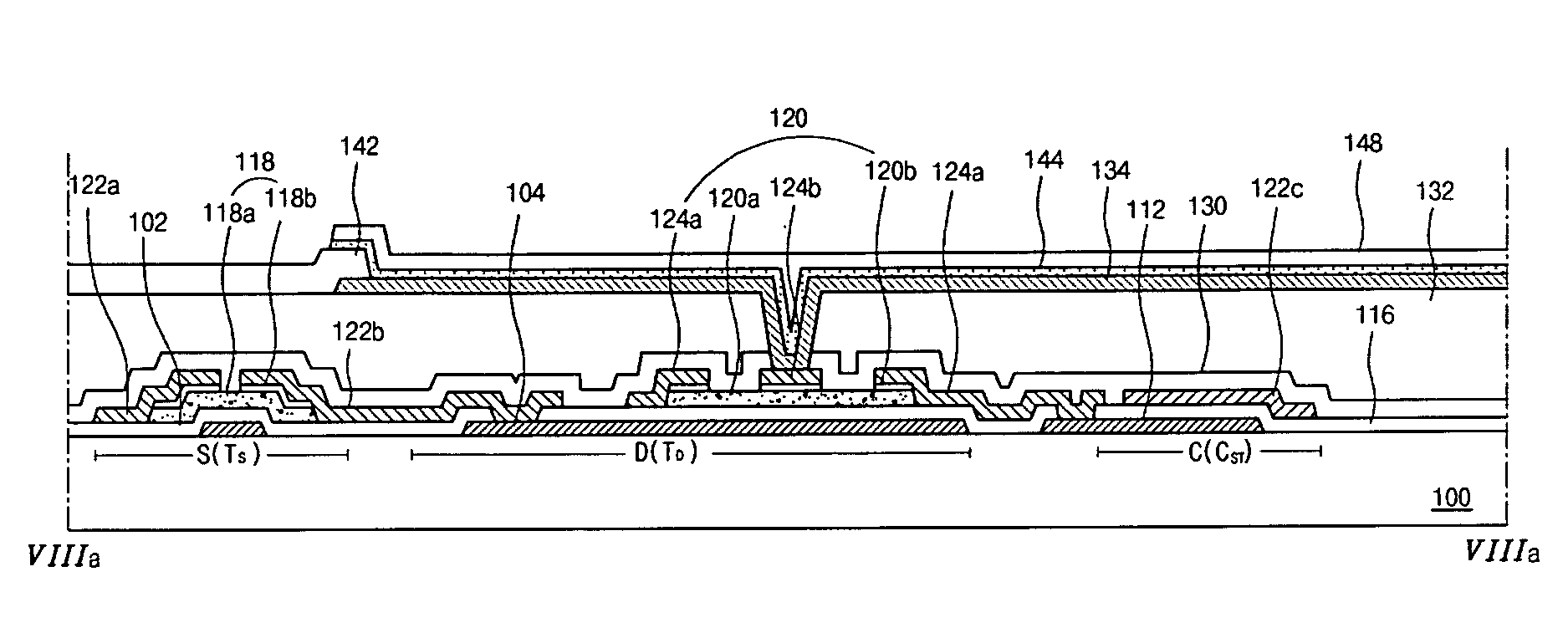
[0048]FIG. 6 is a schematic cross-sectional view of an OELD according to an embodiment of the present invention. As shown in FIG. 6, the OELD “EL” includes an array element (not shown) on a substrate 100, a cathode 200 on the array element, an electron injection layer 202 on the cathode 200, an electron transport layer 204 on the electron injection layer 202, an emitting layer 206 on the electron transport layer 204, a hole transport layer 208 on the emitting layer 206, a hole injection layer 210 on the hole transport layer 208, and an anode 214 over the hole injection layer 210.

[0049]Further, a buffer layer 212 may be disposed between the hole injection layer 210 and the anode 214 to prevent damage to the hole injection layer 210 during a deposition process by sputtering of the anode 214 of ITO or IZO. For example, the buffer layer 212 may include an organic m...


PUM


Abstract

An organic electroluminescent device includes: a switching element and a driving element connected to each other on a substrate including a pixel region; a planarization layer on the switching element and the driving element, the planarization layer having a substantially flat top surface; a cathode on the planarization layer, the cathode connected to the driving element; an emitting layer on the cathode; and an anode on the emitting layer.

Description

[0001]This application claims priority to Korean Patent Application No. 10-2006-059350, filed on Jun. 29, 2006, which is hereby incorporated by reference for all purposes as if fully set forth herein.BACKGROUND OF THE INVENTION[0002]1. Field of the Invention[0003]The present invention relates to an organic electroluminescent device (OELD), and more particularly to a top emission type OELD.[0004]2. Discussion of the Related Art[0005]In general, an OELD emits light by injecting electrons from a cathode and holes from an anode into an emission layer, combining the electrons with the holes, generating an exciton, and transitioning the exciton from an excited state to a ground state. In comparison to a liquid crystal display (LCD) device, an additional light source is not necessary for the OELD to emit light, because the transition of the exciton between the two states causes light to be emitted. Accordingly, the size and weight of the OELD are less than the LCD device.[0006]The OELD has...

Claims


Application Information

Patent Timeline
IPC IPC(8): H05B33/00H01L51/50
CPCH01L27/3244H01L27/3248H01L2251/5315H01L51/50H10K59/123H10K59/12H10K50/00H10K2102/3026H05B33/10H05B33/26
Inventor PARK, JAE-HEEPARK, KYUNG-MINLEE, SEOK-JONG
Owner LG DISPLAY CO LTD
Why Eureka
Try Eureka