
Image processing apparatus and method of controlling image processing apparatus

a technology of image processing apparatus and control apparatus, which is applied in the field of image processing apparatus, can solve the problems of reducing the size of the board, deteriorating the quality of obtained image data, and clock interference between the circuits, and achieve the effect of accurately extracting the beat noise components and eliminating the beat noise components

Inactive Publication Date: 2008-01-17
CANON KK
View PDF9 Cites 8 Cited by
  • Summary
  • Abstract
  • Description
  • Claims
  • Application Information

AI Technical Summary

Benefits of technology

The present invention provides an image processing apparatus and method that can accurately extract beat noise components from an image signal and eliminate them from the image data. This is achieved by a correcting unit that subtracts cyclic data of beat noise from effective pixel data and performs synchronization and phase correction. The invention also allows for offset elimination of beat noise by detecting a parameter minimum value and subtracting it from the parameters of the beat noise. The invention can be used in image processing apparatuses that use A / D converting units and memory units to store and distribute optical black area image data.

Problems solved by technology

With such an imaging apparatus in which a plurality of clock signals having different frequencies exists, there is an unignorable problem in that reduced board sizes due to down-sizing of the apparatus give rise to clock interference between the circuits.
Examples of such interference include interference with a horizontal interval of a clock signal, interference between a horizontal interval of a clock signal and power wiring patterns, and interference between a horizontal interval of a clock signal and analog signals.
An occurrence of such an interference of a clock signal causes frequency noise of the interfering clock signal to be convoluted on captured visual signals, resulting in a problem of deterioration of the quality of obtained image data.
Thus, the conventional example is incapable of handling noise generated in an oblique direction.
In addition, Japanese Patent Laid-Open No. 2002-152600 does not take into consideration a method of processing in a case where the cycle of beat noise signals is not an integral multiple of pixel data.
Therefore, the contents proposed in Japanese Patent Laid-Open No. 2002-152600 are insufficient in handling such a case.
However, elimination of beat noise signals cannot be performed on image data photographed by a multi-field read type solid state image sensor and framed on a memory.

Method used


Image

  • Image processing apparatus and method of controlling image processing apparatus
  • Image processing apparatus and method of controlling image processing apparatus
  • Image processing apparatus and method of controlling image processing apparatus

Examples


first embodiment

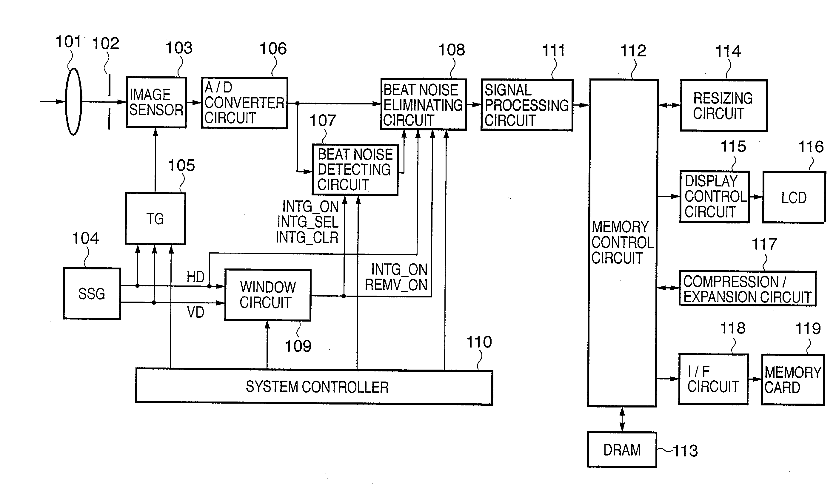
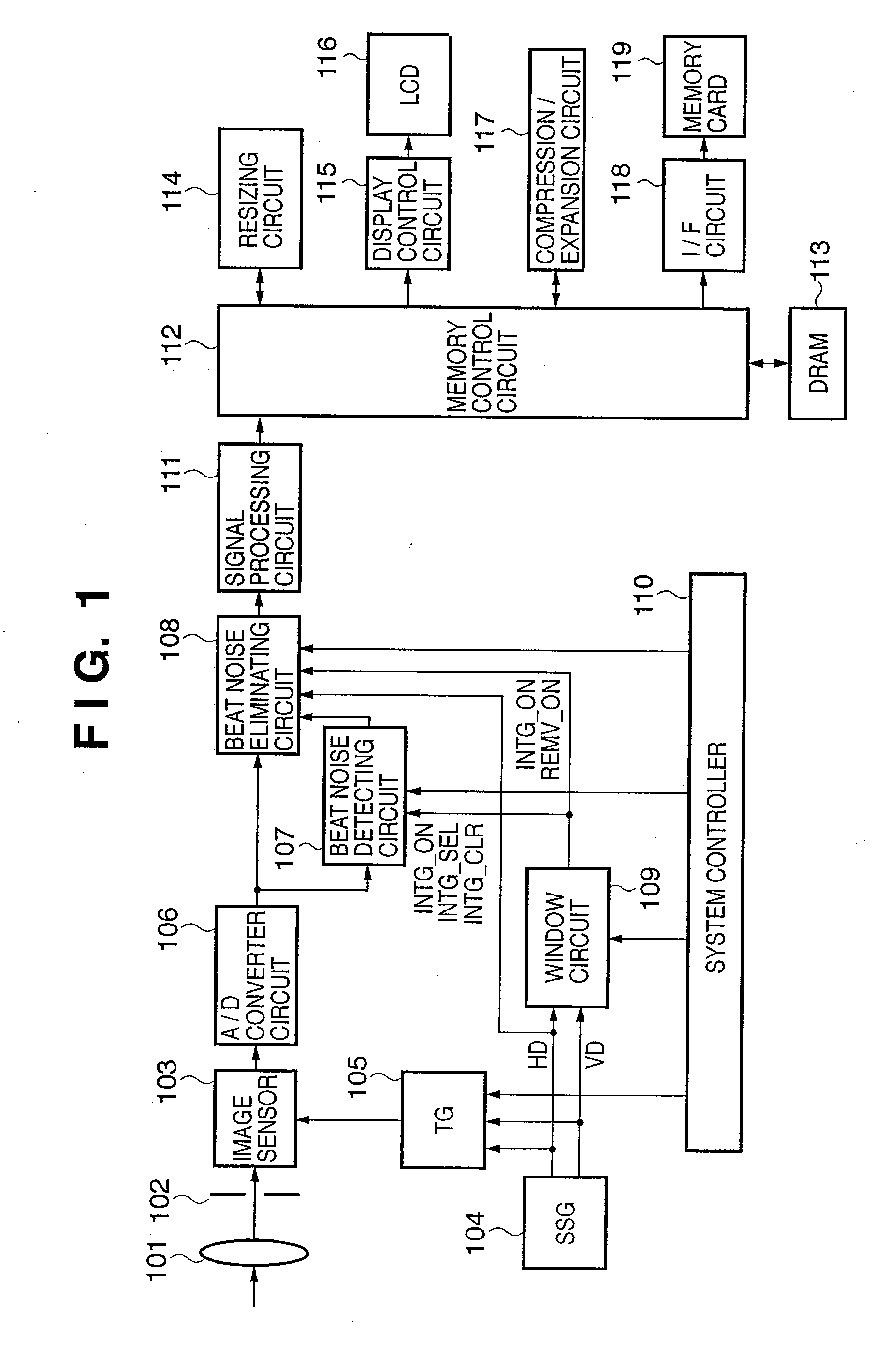
[0036]FIG. 1 is a functional block diagram representing functions of an imaging apparatus that is an image processing apparatus according to a first embodiment of the present invention. The imaging apparatus according to the first embodiment is configured so that the cycle of a beat noise signal is an integral multiple of pixel data, and is configured to be able to eliminate beat noise signals while capturing images.

[0037]In FIG. 1, reference numeral 101 denotes an imaging lens, reference numeral 102 denotes an aperture mechanism, and reference numeral 103 denotes a semiconductor image sensor that photoelectrically converts optical signals. Solid state image sensors based on semiconductor technology, such as CCD image sensors or MOS image sensors, may be used as the image sensor 103. Reference numeral 104 denotes a synchronizing signal generator (hereinafter abbreviated as SSG) that generates a horizontal synchronizing signal HD (hereinafter referred to as HD signal) and a vertical ...

second embodiment

[0065]FIG. 9 is a functional block diagram representing functions of an imaging apparatus that is an image processing apparatus according to a second embodiment of the present invention. The imaging apparatus according to the present second embodiment is configured so that a cycle of a beat noise signal is an integral multiple of a pixel data cycle, and is configured to be able to eliminate beat noise signals by reading out image data from the DRAM 113.

[0066]The imaging apparatus according to the present second embodiment is configured so as to be selectable, by means of a signal outputted by the system controller 110, between beat noise elimination during reading of image data and beat noise elimination on image data read out from the DRAM 113. In addition, even if the beat noise cycle is unknown, beat noise correction may be performed after determining the beat noise cycle by analyzing, through Fast Fourier Transform or the like, an optical black area of read-in image data that is...

third embodiment

[0087]In a third embodiment of the present invention, the beat noise cycle is not an integral multiple of a pixel, and beat noise elimination is performed while acquiring image data. The third embodiment differs from the first in that the beat noise cycle is not an integral multiple of pixel data. A description on portions that differ from the first embodiment will be provided below.

[0088]Circuit configurations and operations of the beat noise detecting circuit 107 and the beat noise eliminating circuit 108 according to the third embodiment will now be described with reference to FIGS. 13A to 13C, 14 and 15.

[0089]FIGS. 13A to 13C are diagrams explaining, in a case where the beat noise cycle is 4.5 pixels, a method of converting 4.5 pixels of optical black pixel data into 5 pixels of noise data that is further used to obtain corrected image data. FIG. 14 is a circuit diagram of the beat noise detecting circuit 107 according to the third embodiment, and FIG. 15 is a circuit diagram of...


PUM


Abstract

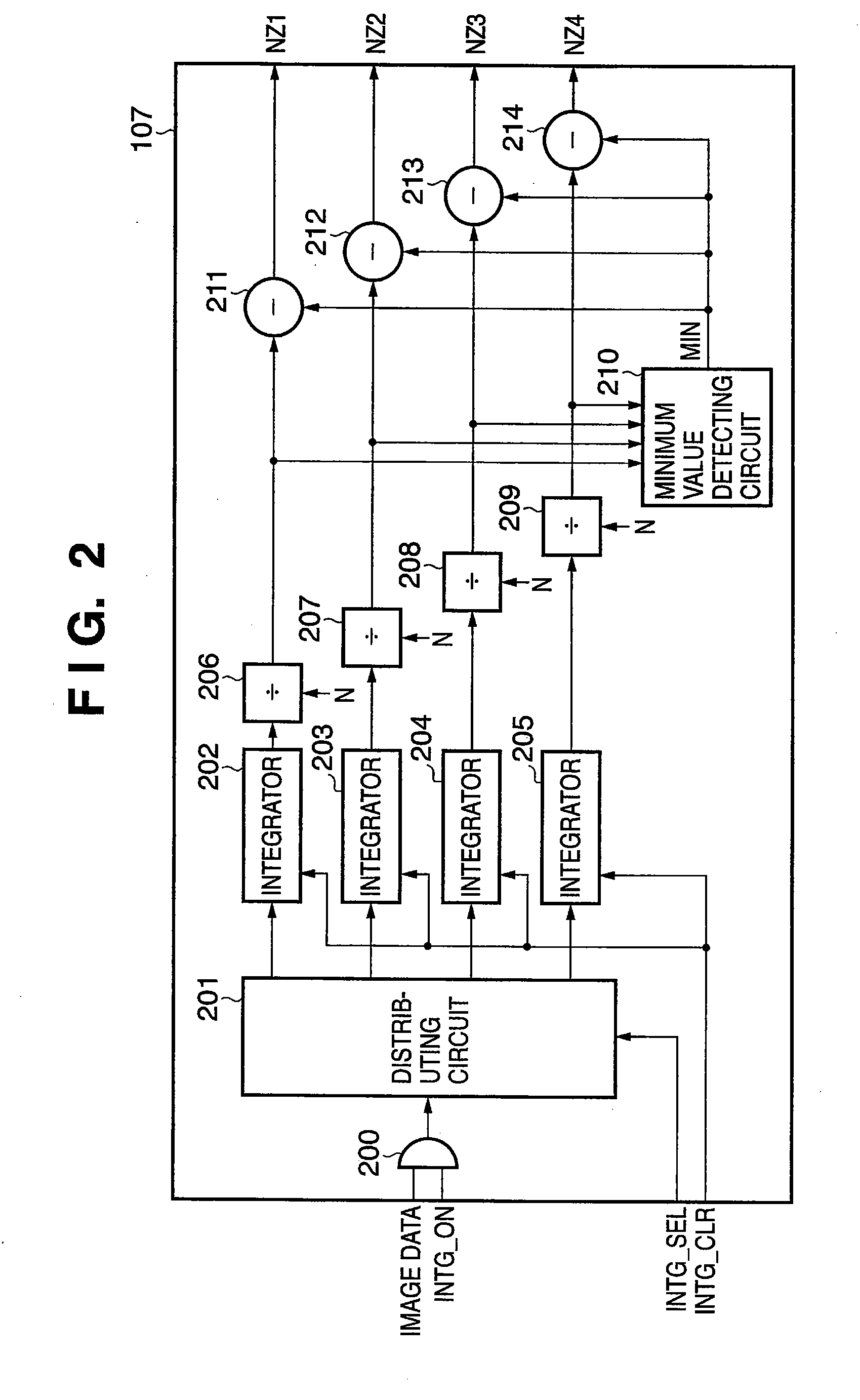
A noise elimination method capable of handling even beat noise occurring in an oblique direction is proposed. In an image processing apparatus that is provided with a correcting unit that subtracts cyclic data of beat noise from effective pixel data included in inputted digital image data, the correcting unit comprises: a distributing unit that sequentially and cyclically distributes optical black area pixel data included in the digital image data; an integrating unit to which the optical black area pixel data distributed by the distributing unit is sequentially inputted; a first calculating unit that divides the integration result of the integrating unit by the number of integrations; a minimum value detecting unit that detects a minimum value of the output of the first calculating unit; and a second calculating unit that calculates the minimum value and the division result to obtain the cyclic data of the beat noise.

Description

BACKGROUND OF THE INVENTION[0001]1. Field of the Invention[0002]The present invention relates to an image processing apparatus and method of controlling an image processing apparatus applicable to an imaging apparatus and the like which captures still images and moving images, and in particular, relates to an image processing apparatus and method of controlling an image processing apparatus capable of eliminating beat noise convoluted on captured visual signals.[0003]2. Description of the Related Art[0004]In recent years, advances have been made in the down-sizing and high-pixelization of solid state image sensors such as CCDs that are used in mobile phones and the like. This has resulted in an increase in the drive frequencies of imaging circuits that drive such solid state image sensors. In addition to a drive circuit for a solid state image sensor, an imaging apparatus includes a control system circuit for a CPU and the like, a memory circuit for a DRAM and the like, as well as a...

Claims


Application Information

Patent Timeline
Patent Type & Authority Applications(United States)
IPC IPC(8): G06K9/40G06T5/00H04N25/00H04N101/00
CPCH04N5/217H04N23/81H04N25/633
Inventor HOHDA, SAORIHARA, TAKAYUKI
Owner CANON KK
Learn More