Screen printing plate

a printing plate and thick film technology, applied in the direction of foil printing, printing, coating, etc., can solve the problems of large number of steps for using organic insulation film, disadvantage in cost, and inability to form through holes

Inactive Publication Date: 2008-01-24
RICOH KK
View PDF12 Cites 72 Cited by
  • Summary
  • Abstract
  • Description
  • Claims
  • Application Information

AI Technical Summary

Benefits of technology

[0009]According to an aspect of the present invention, there is provided a screen printing plate for performing printing by causing a squeegee to be slid to discharge printing liquid. The screen printing plate comprises: a discharging area from which printing liquid is discharged; and a non-discharging area from which no printing liquid is discharged. In the screen printing plate, the non-discharging area is of a polygonal shape having as an apex the point with which the squeegee first comes in contact when being slid, and a width of the non-discharging area in a length direction of the squeegee increases from the apex to a maximum of the width. Accordingly, it is possible to provide the screen printing plate capable of forming minute through-holes in a stable manner.
[0010]According to an embodiment of the present invention, it is possible to provide a screen printing plate capable of forming minute through-holes in a stable manner; a thick film having through-holes, which is formed by the screen printing plate; a multilayer wiring structure having a thick film having the through-holes; and an image display apparatus.

Problems solved by technology

Since photolithography is employed to form through-holes in the organic insulation film, however, using the organic insulation film requires a large number of steps as a manufacturing method and is disadvantageous in terms of cost.
However, it is not suitable for forming minute through-holes.
First, this is because it adopts a dynamic process, resulting in the ink oozing out under the non-discharging area of the screen printing plate at printing being caused to be printed on the substrate.
Second, this is because the surface of fluid ink immediately after the printing becomes even due to gravity, and at the same time, a small amount of feathering is caused to occur (leveling).
In forming minute through-holes, therefore, there is a high probability of the ink oozing out under the non-discharging area at printing and the ink leveling off on all sides after printing filling in the through-holes.
In addition, since the screen printing method is dependent on plural parameters such as clearance (distance between the screen plate and the substrate), the angle, pressure, and speed of the squeegee, it is difficult to form minute through-holes in a stable manner; a through-hole in a large area printing is on the order of 300 μm square using time-proven methods.
However, since the reinforcing linking parts happen to be non-discharging areas, it is not possible to perform screen printing on the entire surface other than the island-shaped parts.

Method used


Image

  • Screen printing plate
  • Screen printing plate
  • Screen printing plate

Examples


example 1

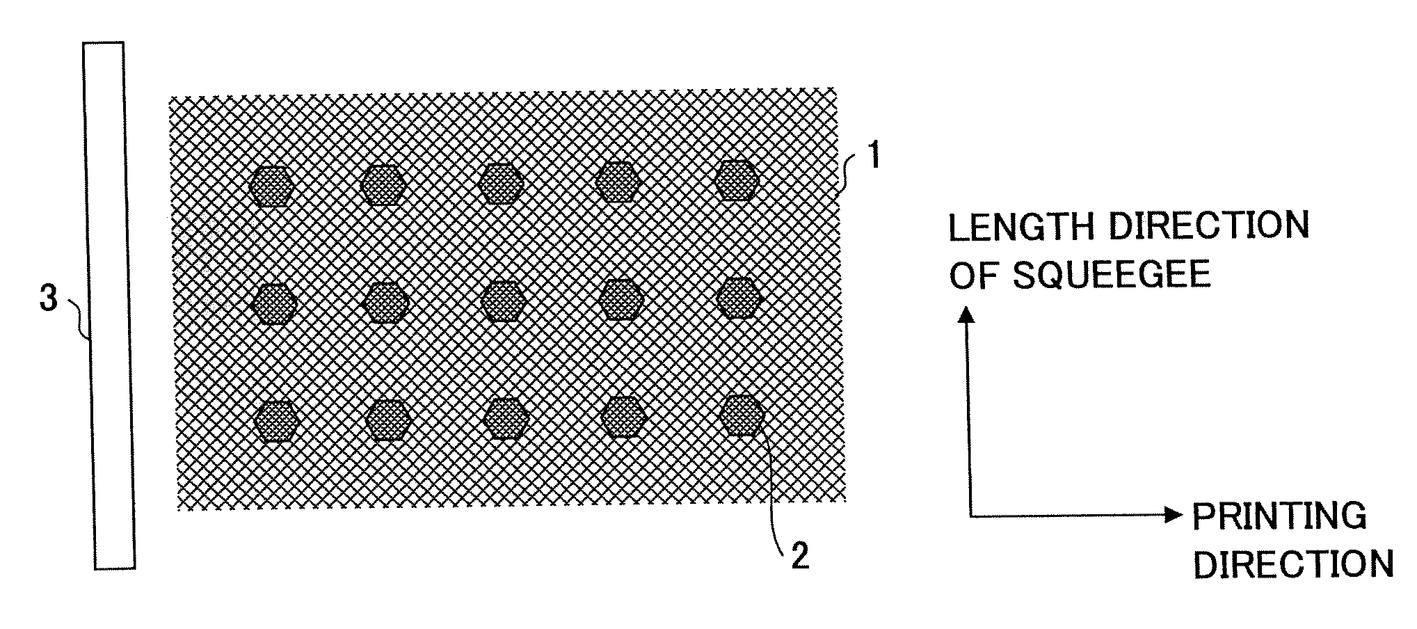
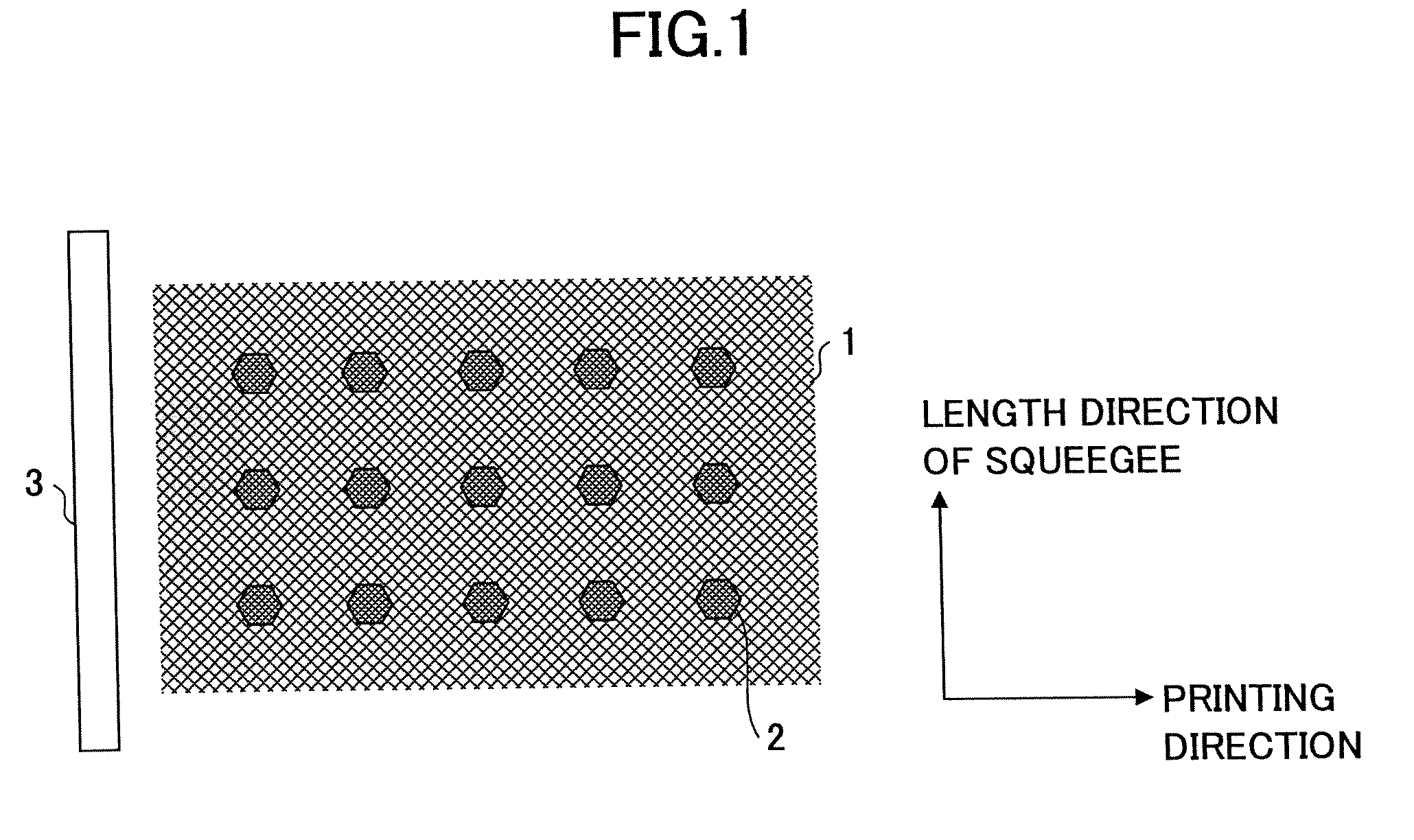
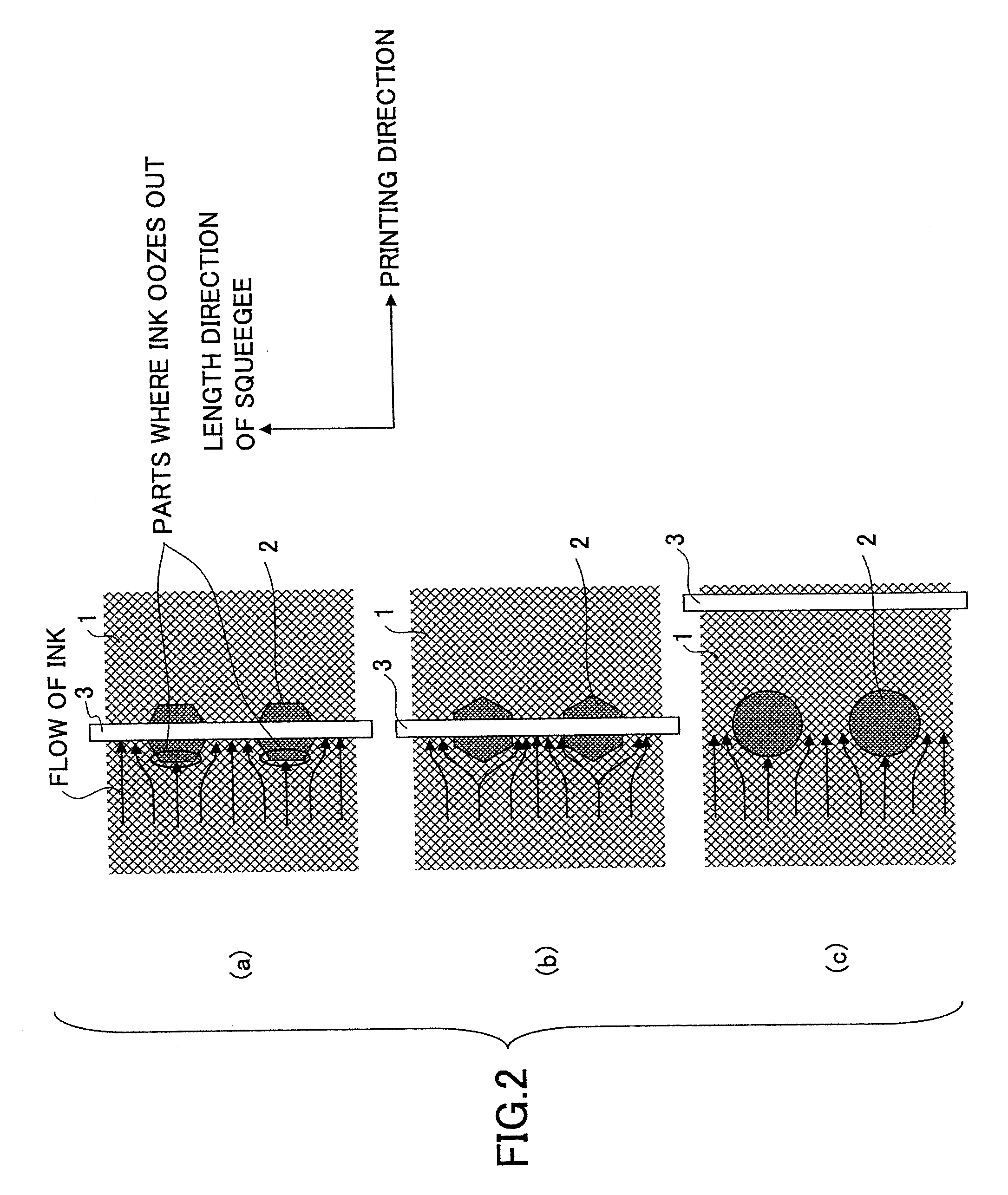
[0042]There was employed, as the screen printing plate, one in which the square through-hole patterns 2, 200 μm on a side, were arranged in a matrix form at intervals of 400 μm (see FIG. 4) on the mesh 1 (200 mm×200 mm) having a wire diameter of 23 μm and an opening ratio of about 50%. Note that the through-hole patterns 2 are axisymmetric with respect to the axis in the printing direction as shown in FIG. 4 and have the apex with which the squeegee first comes in contact. Furthermore, the through-hole patterns 2 were by formed by exposing, developing, and drying a mesh coated with a photosensitive emulsion via a photomask having the through-hole patterns formed thereon.

[0043]After being printed with the screen printing plate and a thick film paste in the printing direction as shown in FIG. 4, a polycarbonate film substrate (220 mm×220 mm) having a thickness of 120 μm was dried for 60 minutes at 100° C. to obtain a thick film. Note that there was employed, as the thick film paste, o...

example 2

[0047]Except that the through-hole patterns 2 of the screen printing plate as shown in FIG. 4 were changed to circular through-hole patterns having a diameter of 200 μm as shown in FIG. 6A, a thick film was formed in the same manner as Example 1. Note that the through-hole patterns are axisymmetric with respect to the axis in the printing direction as shown in FIG. 6A and have the apex with which the squeegee first comes in contact.

[0048]On the entire surface of the obtained thick film, there were formed through-holes having a shape substantially the same as that of the through-hole patterns. The formed through-holes were 160 μm long×160 μm wide on average.

example 4

[0056]Nano-silver ink was formed on a polycarbonate substrate by an ink jet method and then dried to form gate electrodes. Next, a gate insulation film was formed by applying thermal polymerization polyimide thereto by a spin coating method and thermal-treating it at 190° C. The formed gate insulation film had a relative permittivity of 3.6 and a film thickness of 0.4 μm. Ultraviolet rays were applied to the areas, on which source / drain electrodes will be formed via a photomask, to modify the surface of the areas. In addition, nano-silver ink was formed on the areas by the ink jet method and then dried to form the source / drain electrodes. Next, an organic semiconductor material expressed by the structural formula

was dissolved in xylene to form ink. The resulting ink was formed into a film by the ink jet method to form an organic semiconductor layer, thereby obtaining organic transistors. The organic transistors thus obtained had a channel length of 5 μm and a channel width of 2 mm.

[...


PUM


Abstract

A screen printing plate includes a discharging area from which printing liquid is discharged and a non-discharging area from which no printing liquid is discharged. With the screen printing plate, a squeegee is slid to discharge the printing liquid so as to perform printing. The non-discharging area is of a polygonal shape having as an apex the point with which the squeegee first comes in contact when being slid, and a width of the non-discharging area in the length direction of the squeegee increases from the apex to the maximum of the width.

Description

BACKGROUND OF THE INVENTION[0001]1. Field of the Invention[0002]The present invention relates to a screen printing plate, a thick film having through-holes, a multilayer wiring structure, and an image display apparatus.[0003]2. Description of the Related Art[0004]Known semiconductor devices which have transistors and diodes on substrates or semiconductor wafers are of a multilayer wiring structure to enhance their degree of integration. In such a multilayer wiring structure, an interlayer insulation film which includes via-holes for electrical connection of wiring is used.[0005]In recent years and continuing, an organic insulation film having a relative permittivity smaller than that of a silicone dioxide film is widely used as a material of the interlayer insulation film. Since photolithography is employed to form through-holes in the organic insulation film, however, using the organic insulation film requires a large number of steps as a manufacturing method and is disadvantageous...

Claims


Application Information

Patent Timeline
Patent Type & Authority Applications(United States)
IPC IPC(8): B41L13/00
CPCB41M1/12H05K3/1225B41N1/24B41M3/003
Inventor ARAUMI, MAYUKAMURAKAMI, AKISHIGE
Owner RICOH KK
Why Eureka
Try Eureka