Semiconductor Device and Manufacturing Method Thereof

a semiconductor device and semiconductor technology, applied in the direction of semiconductor devices, basic electric elements, electrical appliances, etc., can solve the problems of serious defects in the semiconductor device, high voltage semiconductor devices, etc., and achieve the effect of rapid thermal processing of the semiconductor substra

Active Publication Date: 2008-01-24
DONGBU HITEK CO LTD
View PDF4 Cites 15 Cited by
  • Summary
  • Abstract
  • Description
  • Claims
  • Application Information

AI Technical Summary

Benefits of technology

[0007]A manufacturing method of a semiconductor device having a high voltage region and a low voltage region according to another embodiment comprises: forming a device isolating layer isolating a high voltage region and a low voltage region on a semiconductor substrate; forming a first gate insulating film pattern on the semiconductor substrate in the high voltage region and a first gate electrode on the first gate insulating film pattern, and forming a second gate insulating film pattern on the semiconductor substrate in the low voltage region and a second gate electrode on the second gate insulating film pattern; forming a LDD region by covering the high voltage region with a first photoresist pattern and implanting ions in the low voltage region; removing the first photoresist pattern; forming an insulating film to cover the high voltage region and the low voltage region; forming a second photoresist pattern on the insulating film and covering one side of the first gate electrode and a portion of the semiconductor substrate adjacent the one side thereof and the other side of the first gate electrode and a portion of the semiconductor substrate adjacent the other side thereof; forming a first gate spacer surrounding both sides of the first gate electrode and the portion of the semiconductor substrate and a second gate spacer surrounding both sides of the second gate electrode by etching the insulating film using the second photoresist pattern as a mask; forming a first source and drain region in the high voltage region and the second source and drain region in the low voltage region by ion-implanting over the semiconductor substrate at high concentration; forming a metal film over the semiconductor substrate; and forming a silicide on the first source and drain region, the first gate electrode, and the second source and drain region by performing a rapid thermal processing of the semiconductor substrate.

Problems solved by technology

High voltage semiconductor devices are susceptible to problems where when a photoresist pattern for a silicide blocking pattern is formed at a portion deviating from a designated position, or a dimension of the photoresist pattern is smaller or larger than a designated dimension, the silicide is formed at an unwanted portion, causing a serious defect in the semiconductor device.

Method used


Image

  • Semiconductor Device and Manufacturing Method Thereof
  • Semiconductor Device and Manufacturing Method Thereof
  • Semiconductor Device and Manufacturing Method Thereof

Examples


Embodiment Construction

[0011]Hereinafter, a high voltage semiconductor device according to embodiments of the present invention will be described in more detail with reference to the accompanying drawings.

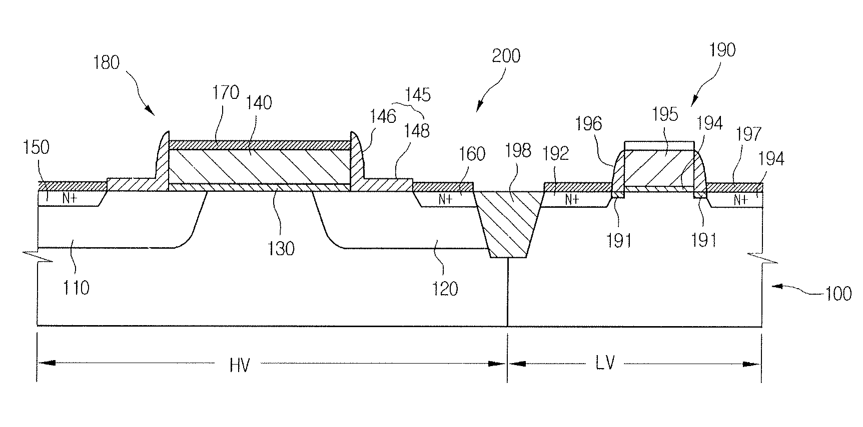
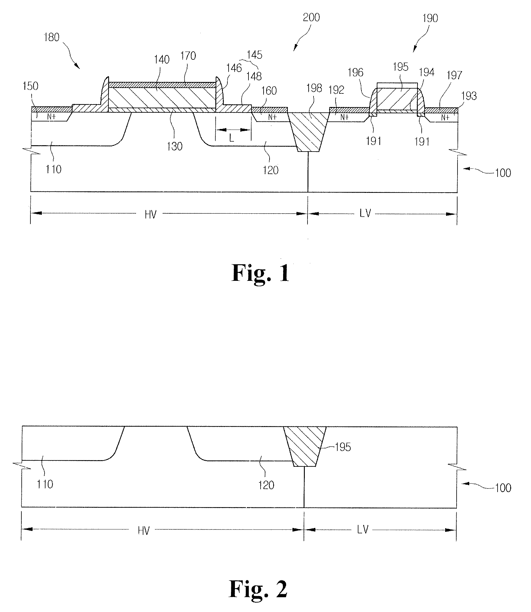
[0012]FIG. 1 is a cross-sectional view showing a high voltage semiconductor device according one embodiment.

[0013]Referring to FIG. 1, the high voltage semiconductor device 200 includes a first conductive type semiconductor substrate 100, a second conductive type drift region 110 and 120, a high voltage gate insulating pattern 130, a high voltage gate electrode 140, a second conductive type high-concentration source 150, a second conductive type high-concentration drain 160, a high voltage gate L-shaped spacer 145, and a silicide 170.

[0014]Referring to FIG. 1, the first conductive type semiconductor substrate 100 can include, for example, a first conductive type well region on a pure silicon substrate, for example, P type impurity such as boron (B), which is group III element can be used as the first con...


PUM


Abstract

A high voltage semiconductor deice and a manufacturing method thereof are provided. The high voltage semiconductor device comprises: second conductive type drift regions disposed spaced from each other on a first conductive type well region formed on a first conductive type semiconductor substrate; a gate electrode on a channel region between the second conductive type drift regions with a gate insulating film disposed therebetween; second conductive type high-concentration source and drain each disposed in the second conductive type drift regions, spaced from a side of a gate electrode; a gate spacer having a spacer part covering the side of the gate electrode and a spacer extending part to cover a spaced portion of the second conductive type high-concentration source and drain from the side of the gate electrode; and a silicide formed on the gate electrode and the second conductive type high-concentration source and drain.

Description

CROSS-REFERENCE TO RELATED APPLICATION[0001]The present application claims the benefit under 35 U.S.C. §119 of Korean Patent Application No. 10-2006-0067601, filed Jul. 19, 2006, which is hereby incorporated by reference in its entirety.BACKGROUND[0002]High voltage semiconductor devices are used for applications in fields such as communication, home appliances, and cars.[0003]High voltage semiconductor devices are susceptible to problems where when a photoresist pattern for a silicide blocking pattern is formed at a portion deviating from a designated position, or a dimension of the photoresist pattern is smaller or larger than a designated dimension, the silicide is formed at an unwanted portion, causing a serious defect in the semiconductor device.BRIEF SUMMARY[0004]Embodiments of the present invention provide a high voltage semiconductor device incorporating a self-aligned silicide. The self-aligned silicide can be formed on the gate electrode and the source and drain regions by ...

Claims


Application Information

Patent Timeline
Patent Type & Authority Applications(United States)
IPC IPC(8): H01L29/78H01L21/336
CPCH01L21/823418H01L21/823443H01L29/665H01L21/823468H01L21/823456
Inventor JUNG, JIN HYO
Owner DONGBU HITEK CO LTD
Why Eureka
Try Eureka