

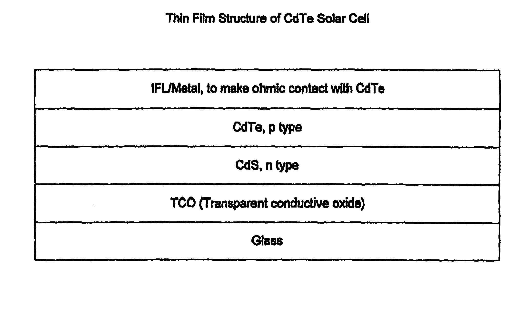
CdTe deposition process for solar cells
a solar cell and cdte technology, applied in the field of cdte deposition of solar cells, can solve the problems of inconvenient in-line processing, time-consuming wet process, and less effective method than cdclsub, so as to facilitate large-scale batch processing of cdte devices, avoid the expense and complexity of wet process, and increase the cdte deposition rate
- Summary
- Abstract
- Description
- Claims
- Application Information
AI Technical Summary
Benefits of technology
Problems solved by technology
Method used
Image

Examples
Embodiment Construction
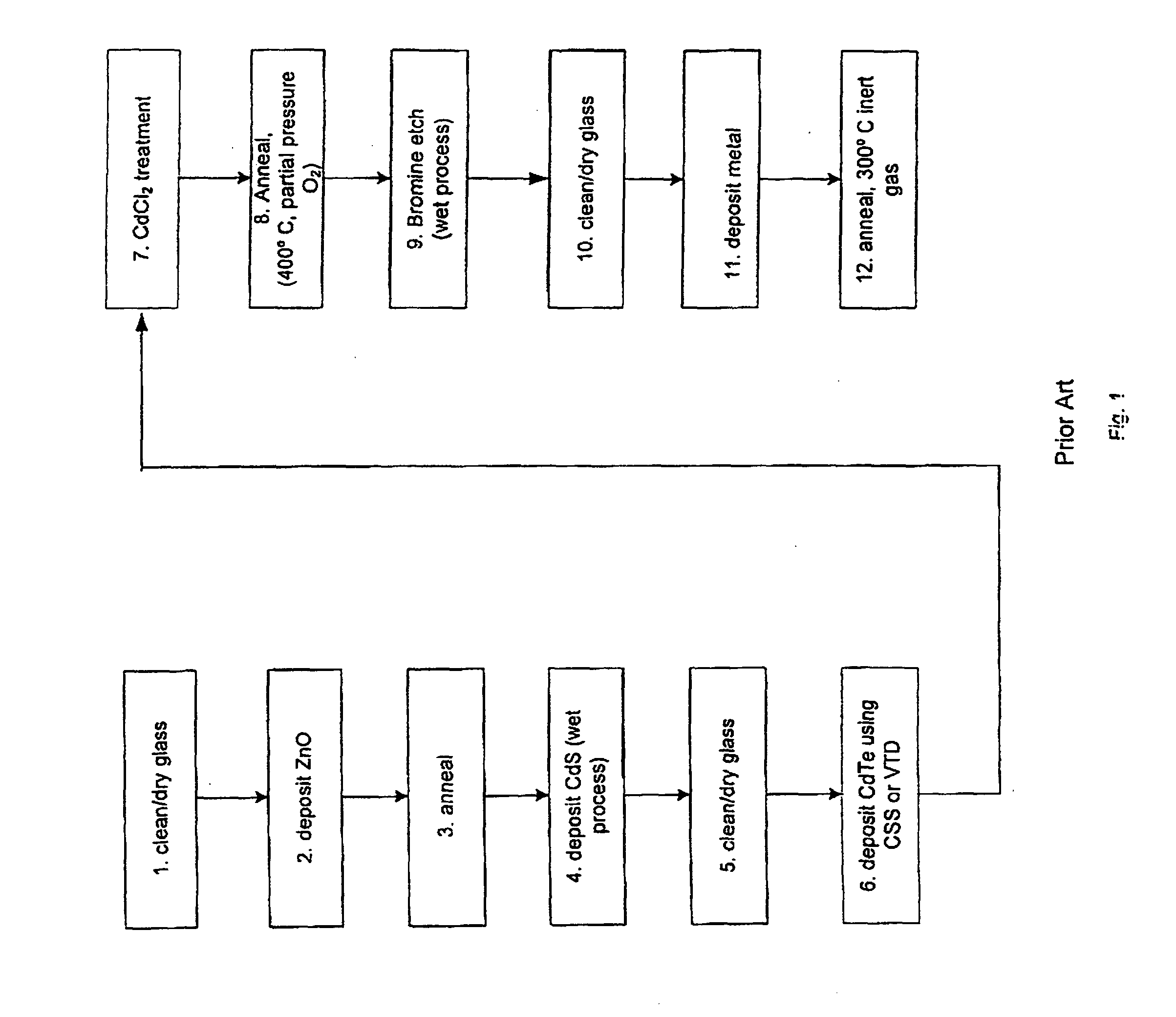
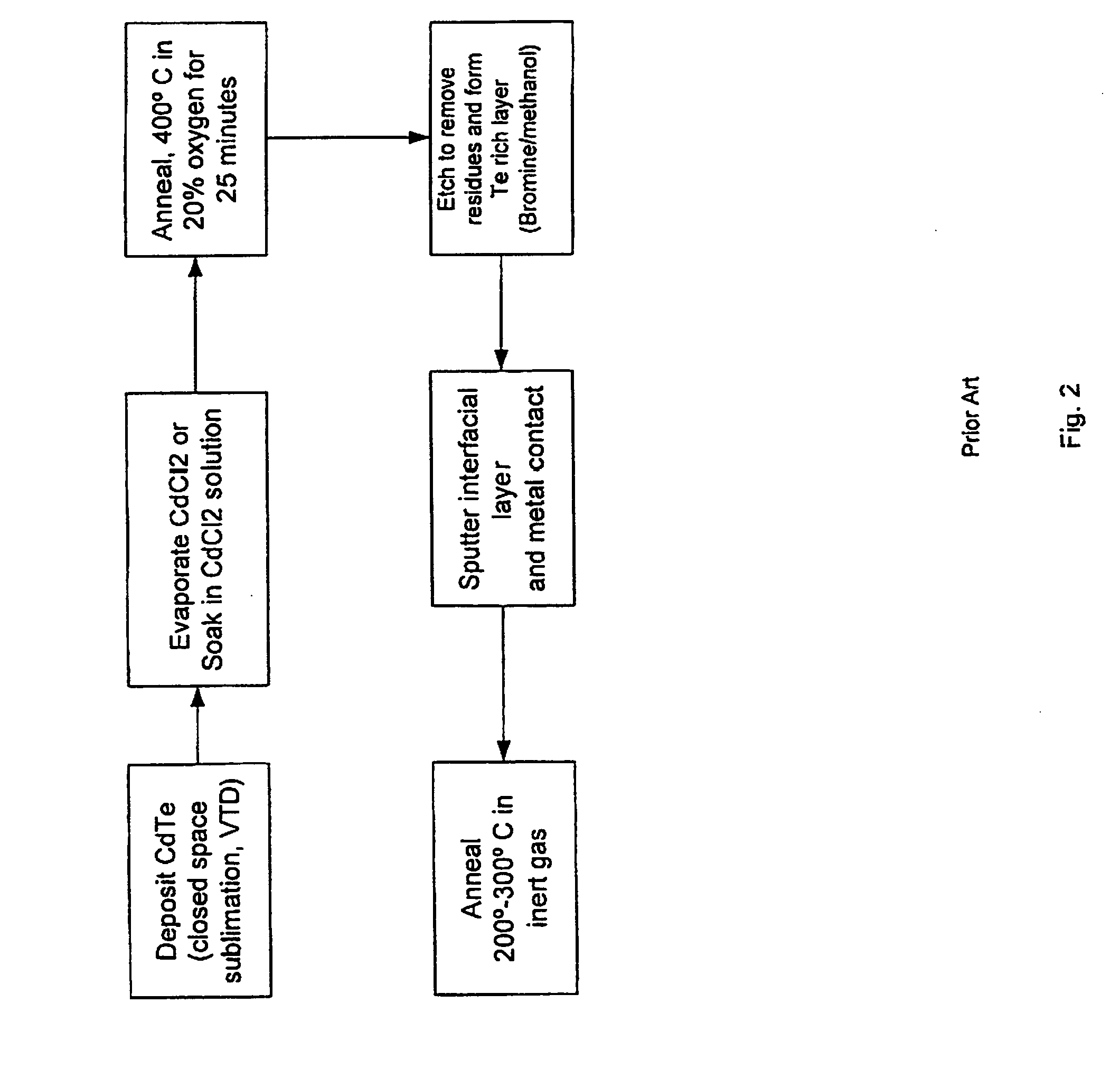
[0024]FIG. 1 shows a conventional method for creating a typical thin film CdTe photovoltaic device. In such a method there are at least three anneal steps and two wet process steps, resulting in undesirable complexity and long processing times. This can greatly increase the cost of a finished CdTe solar cell.
[0025]Referring to FIG. 1, the CdS layer is typically deposited in a wet process such as a chemical bath deposition method (CBD) or a close space sublimation (CSS) method. The thickness of the deposited layer usually is 50 to 200 nm. The CdS layer serves as a window layer and helps to reduce interface recombination with the subsequent CdTe layer.
[0026]After deposition of the CdTe layer, conventional processing technologies usually include a post deposition heat treatment with CdCl2 that is annealed at 400° C. as shown. The CdCl2 treatment has been shown to increase grain size.
[0027]A final step in the cell fabrication in the conventional process of FIG. 1 is the application of t...
PUM
 Abstract
Description
Claims
Application Information