Microwave hybrid and plasma rapid thermal processing of semiconductor wafers

a technology of plasma rapid thermal processing and semiconductor wafers, which is applied in the direction of electric/magnetic/electromagnetic heating, electric discharge tubes, electrical equipment, etc., can solve the problem of inability to achieve fast heating rates of several hundred degrees/min, and achieve the effect of rapid thermal processing of semiconductor wafers

Inactive Publication Date: 2008-08-28
BTU INTERNATIONAL
View PDF6 Cites 13 Cited by
  • Summary
  • Abstract
  • Description
  • Claims
  • Application Information

AI Technical Summary

Benefits of technology

[0005]Microwave energy is used as a radiation source for rapid thermal processing of semiconductor wafers and other substrates capable of absorbing microwaves.

Problems solved by technology

Using a conventional furnace, fast heating rates on the order of several hundred degrees / min cannot be achieved.

Method used


Image

  • Microwave hybrid and plasma rapid thermal processing of semiconductor wafers
  • Microwave hybrid and plasma rapid thermal processing of semiconductor wafers
  • Microwave hybrid and plasma rapid thermal processing of semiconductor wafers

Examples


Embodiment Construction

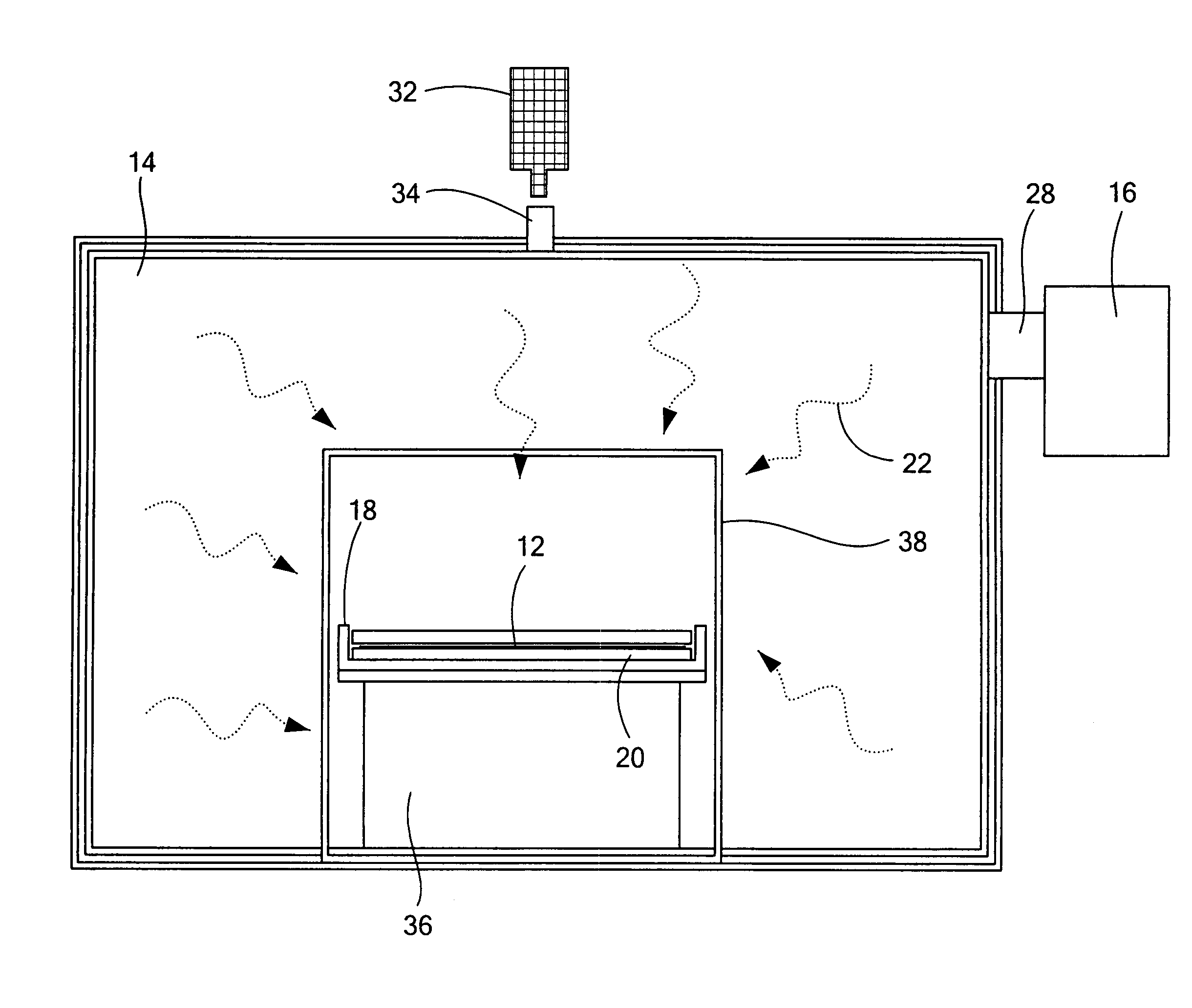
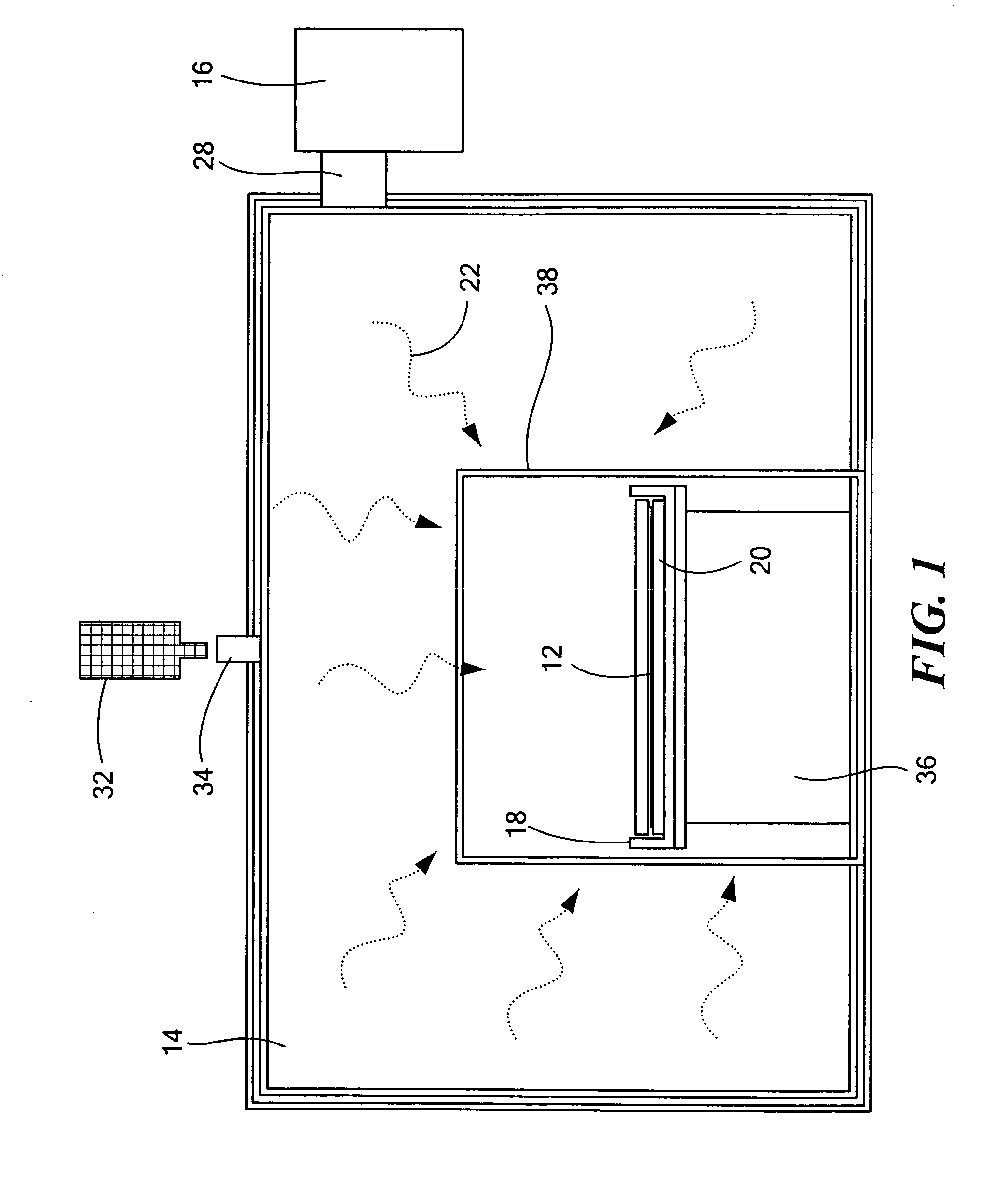
[0019]In one aspect of the present invention, a hybrid microwave rapid thermal processing (RTP) method of heating a wafer, for example, a Si wafer, is described generally with reference to FIG. 1. The wafer 12 to be heated is located within a microwave cavity 14 provided with a microwave radiation source (for example, at 2.45 GHz) to heat the wafer. The wafer is also in thermal communication with a hybrid material 18 formed from a suitable microwave modulator material, such as SiC. The hybrid material distributes heat uniformly to the wafer, preventing thermal shock, which could cause cracking or breakage of the wafer, both during heating and cooling. A buffer or insulation layer 20 is placed between the hybrid material and the wafer or underlying support pedestal if necessary to prevent diffusion of the hybrid material into the wafer and / or the pedestal. For example, SiC from the hybrid material can diffuse C species into a Si wafer. Quartz forms a suitable buffer layer, because it...


PUM


Abstract

Microwave energy is used as a radiation source for rapid thermal processing of semiconductor wafers. In one aspect, a hybrid material formed from a microwave modulator material is used to provide temperature uniformity across the wafer and to avoid cracking or breaking of wafers due to the development of thermal stresses. In another aspect, microwave-generated atmospheric pressure plasma is used to heat the wafer either directly or indirectly.

Description

CROSS REFERENCE TO RELATED APPLICATIONS[0001]This application claims the benefit under 35 U.S.C. § 119(e) of U.S. Provisional Patent Application No. 60 / 897,450, filed Jan. 25, 2007, the disclosure of which is incorporated by reference herein.STATEMENT REGARDING FEDERALLY SPONSORED RESEARCH OR DEVELOPMENT[0002]N / ABACKGROUND OF THE INVENTION[0003]Rapid thermal processing (RTP), employing heating rates on the order of hundreds of degrees per minute, is used in the semiconductor industry wherever a low thermal budget is preferred. For example, a low thermal budget is desired in ultra-small IC manufacturing processes to prevent dopant redistribution. Similarly, in the electronic industries, RTP finds an application in very large scale integration (VLSI) processes, in which the growth of ultra thin gate oxides and activation annealing of ion implanted species are usually done by RTP. In the photovoltaic (PV) industry, RTP is useful for many different purposes, such as phosphorous (P) dopi...

Claims


Application Information

Patent Timeline
Patent Type & Authority Applications(United States)
IPC IPC(8): H01L21/324H05B6/64
CPCH01J37/32192H01L21/67115H01J37/32825H01L21/00H01L21/324
Inventor PEELAMEDU, RAMESHWONG, DAVID C.
Owner BTU INTERNATIONAL
Why Eureka
Try Eureka