Composite metallization process for filling high aspect ratio contact holes

a technology of composite metallization and contact hole, which is applied in the direction of semiconductor devices, semiconductor/solid-state device details, electrical equipment, etc., can solve the problems of yield or reliability problems, the contact hole diameter is more difficult to fill using conventional metal deposition procedures than the diameter of the contact hole with the larger opening, and the conventional sputtering process has difficulty in adequately filling the contact hol

Inactive Publication Date: 2001-11-29
YANG CHI CHENG +1
View PDF0 Cites 12 Cited by
  • Summary
  • Abstract
  • Description
  • Claims
  • Application Information

AI Technical Summary

Problems solved by technology

For example, sub-micron diameter contact holes used to connect wiring metallizations to underlying silicon regions are more difficult to fill using conventional metal deposition procedures than are contact holes with larger diameter openings.
As the aspect ratio of contact holes increases, conventional sputtering processes have difficulty in adequately filling the contact holes.
Incomplete metal fills can lead to yield or relia

Method used


Image

  • Composite metallization process for filling high aspect ratio contact holes
  • Composite metallization process for filling high aspect ratio contact holes
  • Composite metallization process for filling high aspect ratio contact holes

Examples


Embodiment Construction

.

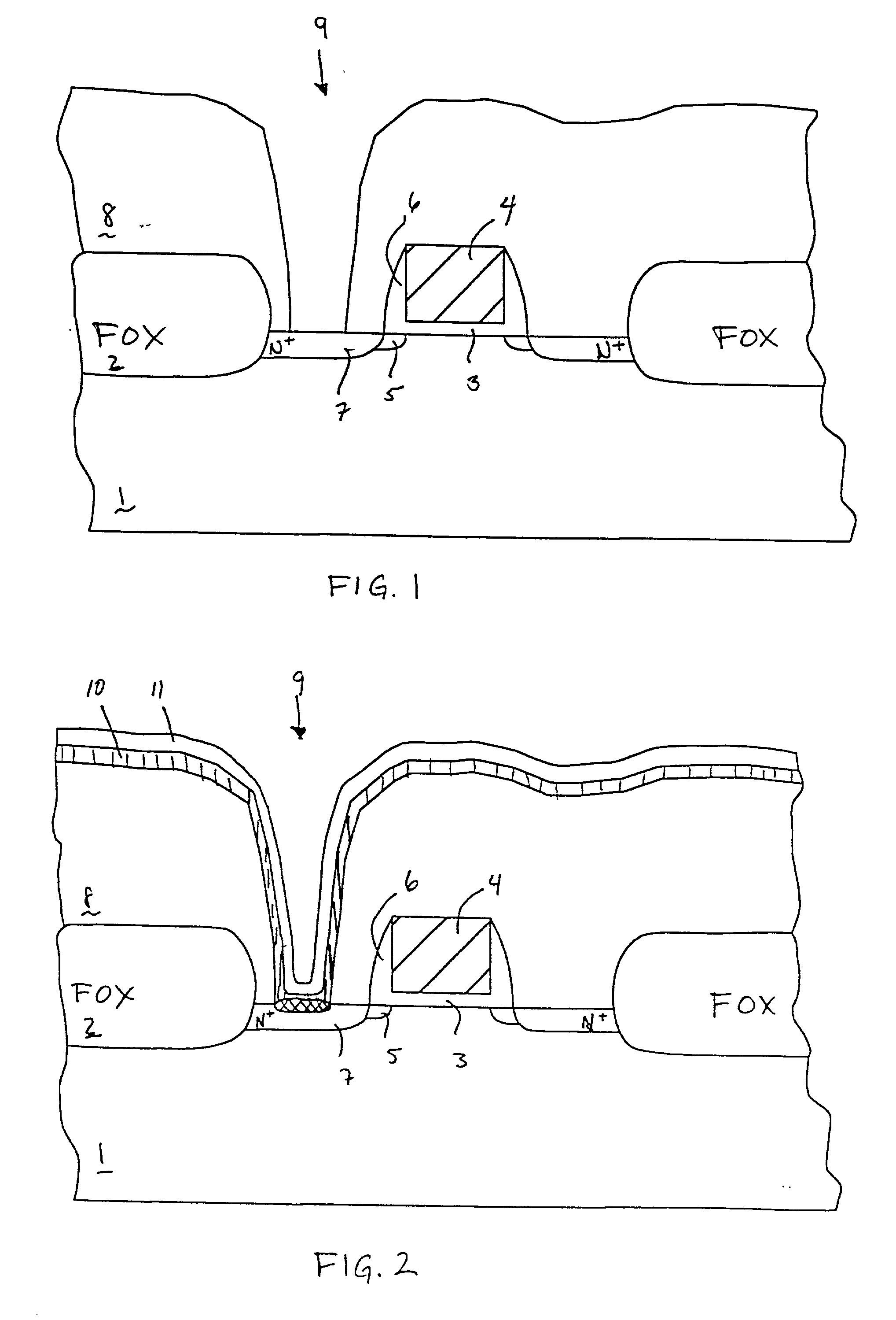
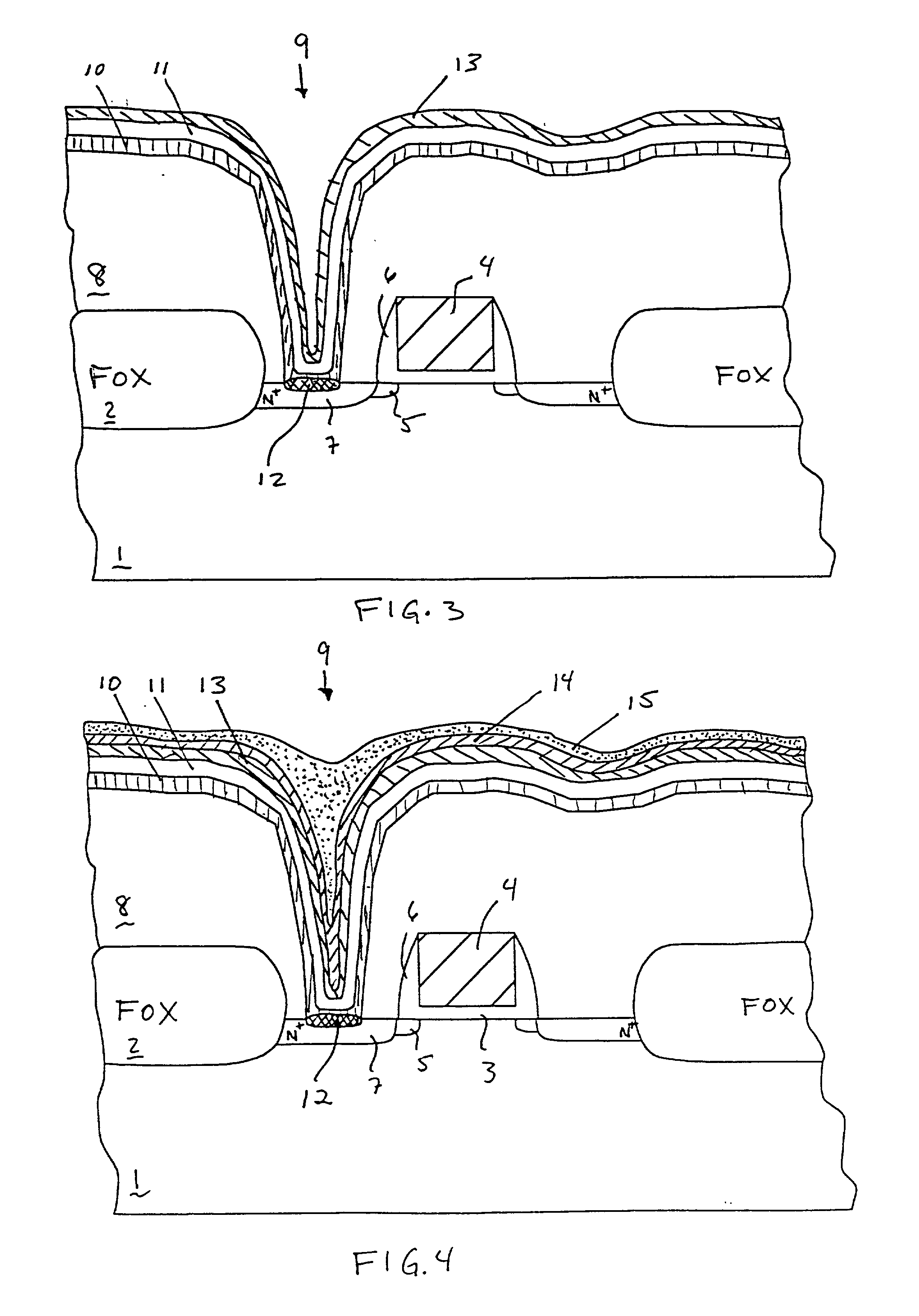
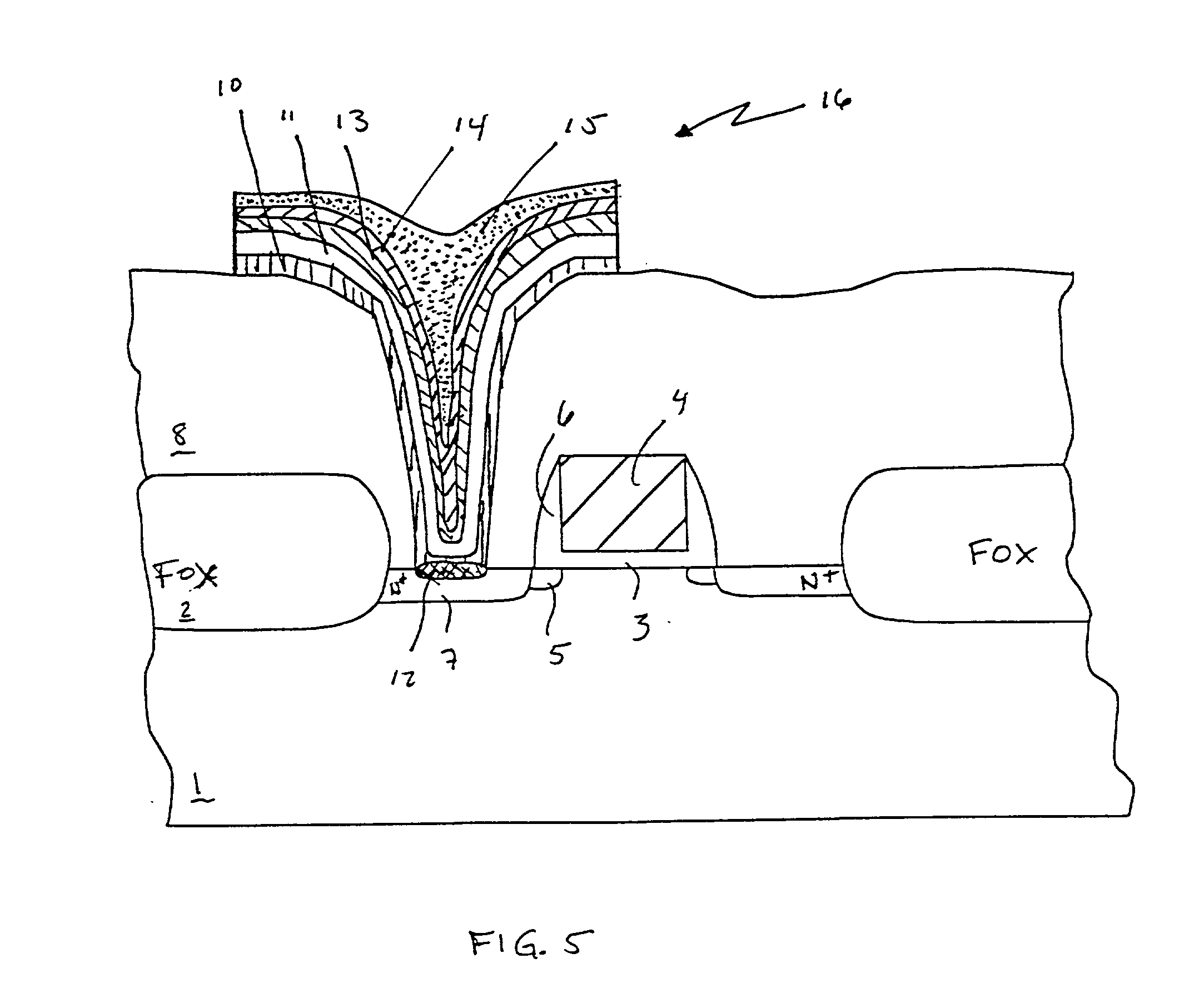
[0009] Aspects of the present invention include an improved process for deposition of metal contact films including an underlying layer of titanium, preferably formed using a collimated deposition process, to provide a better surface for cold aluminum adhesion. This invention will also describe a two step aluminum sputtering process, resulting in optimum metal filling of high aspect ratio contact holes, with the hot deposition stage being performed at a temperature high enough to form an intermetallic layer of Ti.sub.xAl.sub.y, again resulting in improved adhesion between the aluminum fill and underlying materials.

[0010] One aspect of this invention provides a method of depositing a composite metallization that results in successful filling of high aspect ratio contact holes.

[0011] Another aspect of this invention uses an underlying adhesion layer as part of the composite metallization layer to provide wettability for subsequent layers of the composite metallization layer.

[0012] Ye...


PUM


Abstract

A process has been developed in which high aspect ratio contact holes can be successfully filled, without voids, using a composite metallization layer. After adhesive and barrier layers are deposited, an additional titanium adhesive layer is deposited, for purposes of improving the adhesion of subsequent, overlying metallizations to underlying device structures. A two step aluminum deposition process is then employed, using an initial cold deposition followed by a hot aluminum deposition. The hot aluminum deposition process results in complete filling of the high aspect ratio contact hole, and also allows the formation of a titanium-aluminum intermetallic layer at the interface of the titanium adhesive layer and the initial, cold aluminum deposition layer.

Description

[0001] This application claims priority from provisional application Ser. No. 60 / 009,355, filed Dec. 29, 1995.[0002] 1. Field of the Invention[0003] The present invention relates to the methods used to fabricate semiconductor devices, and more specifically to methods used to form metal contacts.[0004] 2. Description of the Related Art[0005] The semiconductor industry is continually striving to improve the performance of silicon devices. The trend to miniaturization, resulting in silicon devices with sub-micron features, has improved performance. Reductions in critical device features translate to decreases in device resistances and capacitances, which in turn result in performance benefits. The attainment of submicron features has in part been realized by advances in specific semiconductor fabrication disciplines, such as photolithography and dry etching. For example, more advanced exposure cameras, as well as development of more sensitive photoresist materials, have allowed sub-mic...

Claims


Application Information

Patent Timeline
IPC IPC(8): H01L21/768H01L23/532
CPCH01L21/76843H01L21/76846H01L21/76855H01L21/76856H01L21/76858H01L2924/0002H01L21/76877H01L23/53223H01L2924/00
Inventor YANG, CHI-CHENGLIN, JENN-TARNG
Owner YANG CHI CHENG
Why Eureka
Try Eureka