Photomask, and method and apparatus for producing the same

a technology of photomasks and masks, applied in the field of photomasks, can solve the problems of serious effect of arrangement errors of shading portions on the arrangement, shape or dimension of patterns transferred onto semiconductor substrates, and achieve the effect of large working accuracy tolerance margins

Inactive Publication Date: 2008-01-24
RENESAS ELECTRONICS CORP
View PDF5 Cites 4 Cited by
  • Summary
  • Abstract
  • Description
  • Claims
  • Application Information

AI Technical Summary

Benefits of technology

[0015] An object of the present invention is to provide a photomask making it possible to make large the working accuracy tolerance margin of the correction portion of a defect in defect correction of an HT mask, a method for producing the photomask, and an apparatus for producing the photomask.
[0017] According to the above-mentioned aspect, the adjustment of the arrangement and the transmissivity of the semitransparent portion formed in a defect potion and in the vicinity thereof makes it possible to correct the photomask in such a manner that a corrected pattern is transferred onto a semiconductor substrate so as to be approximately a complete pattern.
[0019] However, the effect of an arrangement error of the semitransparent portion on the pattern transferred onto a semiconductor substrate is smaller than the effect of the arrangement error of the shading portion on the arrangement, shape or dimension of the pattern transferred onto a semiconductor substrate. Accordingly, the margin of the arrangement of the semitransparent portion can be made larger than the margin of the arrangement of the shading potion.
[0020] As a result, in the case where the photomask with its clear defect portion corrected by the semitransparent portion is used to transfer a pattern corresponding to the clear defect portion, onto a semiconductor substrate, the rate of occurence of dimensional fluctuation of the transferred pattern on the semiconductor substrate can be made small. Accordingly, the yield of semiconductor devices can be improved.

Problems solved by technology

In general, in the case that the adjustment of the arrangement of a shading portion having a transmissivity of about 0% causes a pattern approximate to the complete pattern to be transferred onto a semiconductor substrate, an arrangement error of the shading portion produces a serious effect on the arrangement, shape or dimension of the pattern transferred onto the semiconductor substrate.

Method used


Image

  • Photomask, and method and apparatus for producing the same
  • Photomask, and method and apparatus for producing the same
  • Photomask, and method and apparatus for producing the same

Examples


first embodiment

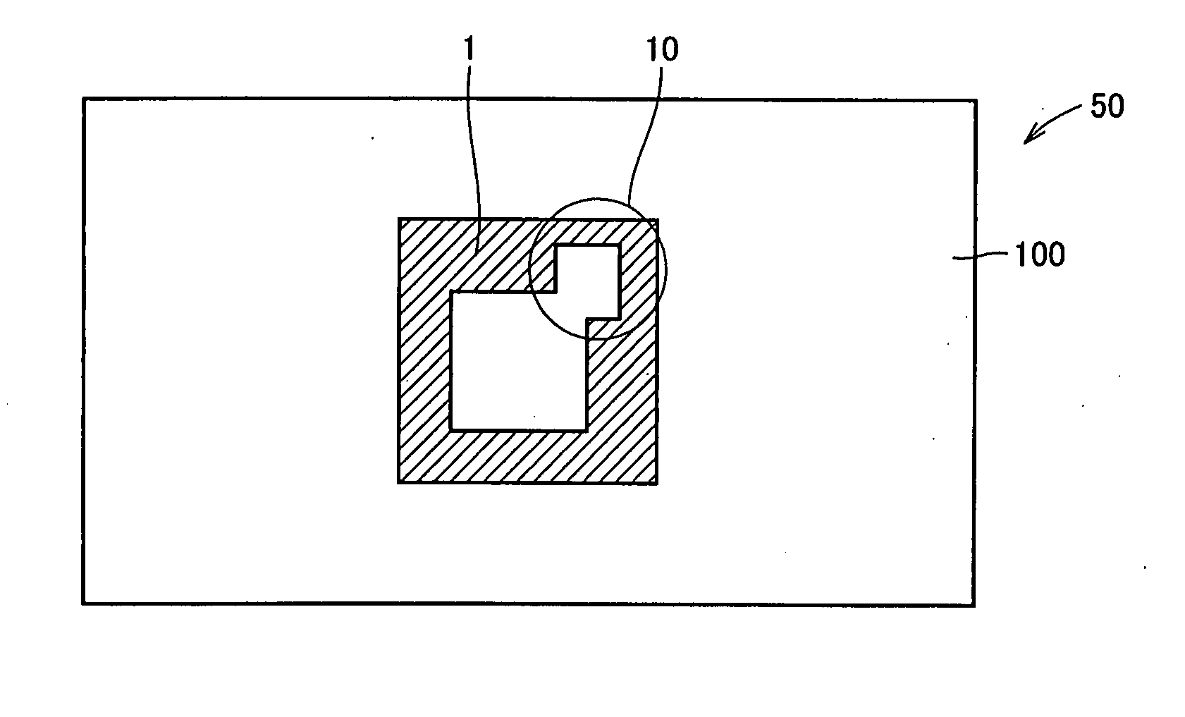
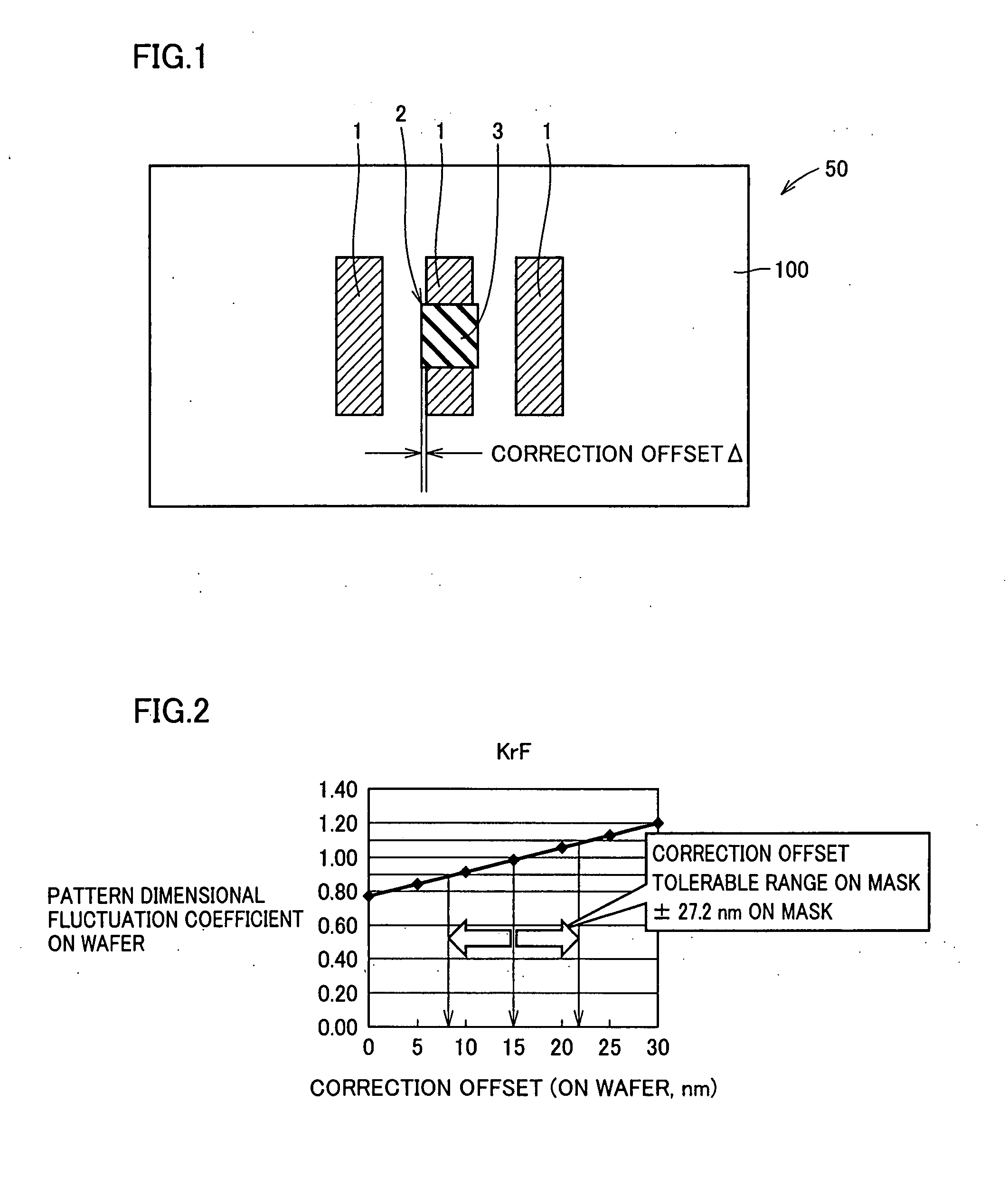
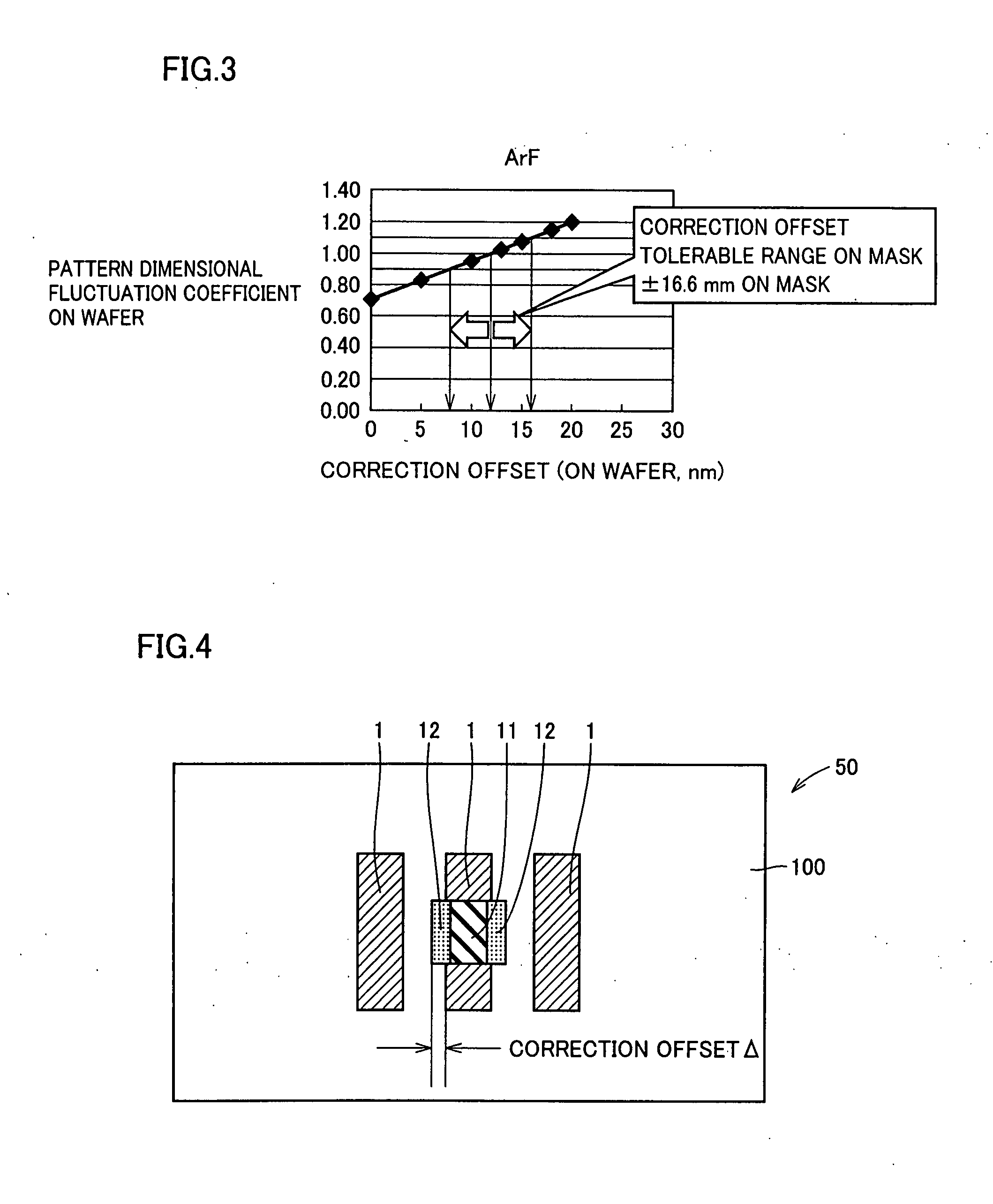
[0069] In order to compare the method for correcting a photomask according to the present embodiment with a method for correcting a photomask according to a comparative embodiment, the method for correcting a photomask according to the comparative embodiment will be specifically described. An HT mask as the photomask used in this correcting method according to the comparative embodiment will be described referring to FIG. 1. In this photomask, a wire-breaking defect, which is one example of clear defects, generated in a wiring pattern on the HT mask is corrected, as illustrated in FIG. 1.

[0070] The HT mask illustrated in FIG. 1 is used at an exposure wavelength of 284 nm. This HT mask is composed of wiring patterns 1 (semitransparent film) having a width of 0.52 μm and space patterns formed between wiring patterns 1 in such a manner that the ratio between their widths is 1 / 1. In the method for correcting a defect according to the comparative embodiment, the portion of the defect is...

second embodiment

[0097] The following will describe a method for correcting a hole pattern of a photomask according to a second embodiment. In the photomask correcting method of the present embodiment, the same manner as in the photomask correcting method of the first embodiment is used except that a pattern to be corrected is different.

[0098]FIGS. 20 and 21 illustrate a state that in an HT mask used at an exposure wavelength of 248 nm, a clear defect (edge missing defect having a dimension of about 0.3 μm) is formed at an edge of a hole pattern about 0.6 μm square.

[0099] In the method of using a carbon film to correct a clear defect according to the comparative embodiment, in order to make the tolerable range of the dimensional fluctuation of the pattern, on a wafer, obtained after a clear defect corrected portion is transferred, into the range of ±10% of a target dimension, it is necessary that the tolerable location of carbon film 3 formed on the photomask is within the range of ±68 nm (span: 1...

third embodiment

[0103] The following will describe the photomask correcting method of the first or second embodiment in more detail.

[0104]FIG. 25 shows results measured in the case that Ga ions are radiated onto the surface of transparent substrate 100 made of quartz as a mask material by means of an FIB radiating apparatus wherein the accelerating voltage thereof is 30 KeV, and shows change in the light transmissivity of a portion onto which Ga ions are radiated when the total dose of the Ga ions is changed. As the radiated ions, ions of Au, Si or Be may be used instead of the Ga ions. In, Pb or Zn may be used instead of Ga if the problem of difficulty in the use thereof is overcome.

[0105] As illustrated in FIG. 25, the dose of radiated Ga ions is increased from 0 to 0.2 nC / μm2, the transmissivity of transparent substrate 100 is gradually lowered. For example, the transmissivity of the surface of transparent substrate 100 onto which Ga ions are radiated at a dose of 0.1 nC / μm2 is 22% when the wa...


PUM

PropertyMeasurementUnit
thicknessaaaaaaaaaa
sizeaaaaaaaaaa
sizeaaaaaaaaaa

Abstract

A shading area having a transmissivity in the range of 0 to 2% is formed at the center of a clear defect in a wiring pattern of a halt half tone mask. Semitransparent areas having a transmissivity in the range of 10 to 25% are formed, adjacently to shading area, in areas extending from the inside of the edge of an imaginary pattern having no defect to the outside of the edge. In this way, in the correction of the defect in the half tone mask, the working accuracy tolerable margin of the correction portion of the defect can be made large.

Description

[0001] This application is a Continuation of U.S. application Ser. No. 10 / 714,362, filed Nov. 17, 2003, claiming priority of Japanese Application No. 2003-024125, filed Jan. 31, 2003, the entire contents of each of which are hereby incorporated by reference.BACKGROUND OF THE INVENTION [0002] 1. Field of the Invention [0003] The present invention relates to a photomask used in a lithographic process, a method for producing the same, and an apparatus for producing the same. [0004] 2. Description of the Background Art [0005] Hitherto, a photomask wherein a shading pattern (semitransparent film) is formed on a surface of a transparent substrate has been used in the lithographic step for semiconductor devices. In the shading film pattern of this photomask, a clear defect such as a pattern chipping or a pinhole may be generated. [0006] In this case, a focused ion beam (FIB) is radiated onto the clear defect in the atmosphere of organic gas, thereby correcting the clear defect. According t...

Claims


Application Information

Patent Timeline
Patent Type & Authority Applications(United States)
IPC IPC(8): G03F9/00G06K9/00G03F1/72G03F1/74G03F7/00G03F7/20H01L21/027
CPCG03F1/74G03F1/32G03F1/72
Inventor NAGAMURA, YOSHIKAZUTANGE, KOUJIHAYASHI, KOUKIIKEDA, HIDEHIRO
Owner RENESAS ELECTRONICS CORP
Why Eureka
Try Eureka