Layout method and semiconductor device

Inactive Publication Date: 2008-01-24
PANASONIC CORP
View PDF2 Cites 65 Cited by
  • Summary
  • Abstract
  • Description
  • Claims
  • Application Information

AI Technical Summary

Benefits of technology

[0033]In the cell group constituted based on the conditions described above, the variation is small in the process variation and furthermore the size of the cell group is small. Moreover, since the dummy element is unnecessary for each cell, an area increase is controlled while improving the relative configuration accuracy.
[0034]According to the present invention, after aligning the plural cells at equal intervals, the inter-cell distance is equalized to the intra-cell distance. Therefore, the whole situation variation can be made constant, and the output characteristic of plural terminals can be made uniform without generating increase of the area and complexity of the circuit instead of insertion of the dummy element in an individual cell.
[0035]Whe

Problems solved by technology

This is because the density and the distance of the polysilicon are different in the layout arrangement, and because the factor of the whole situation variation is complex and large.
In this case, the cell size is difficult to calculate accurately except for a termination phase of the circuit design.
Additionally, there is a possibility of causing the degradation of the relative configuration accuracy when the distance between transistors is adjusted for reduction of area

Method used


Image

  • Layout method and semiconductor device
  • Layout method and semiconductor device
  • Layout method and semiconductor device

Examples


first embodiment

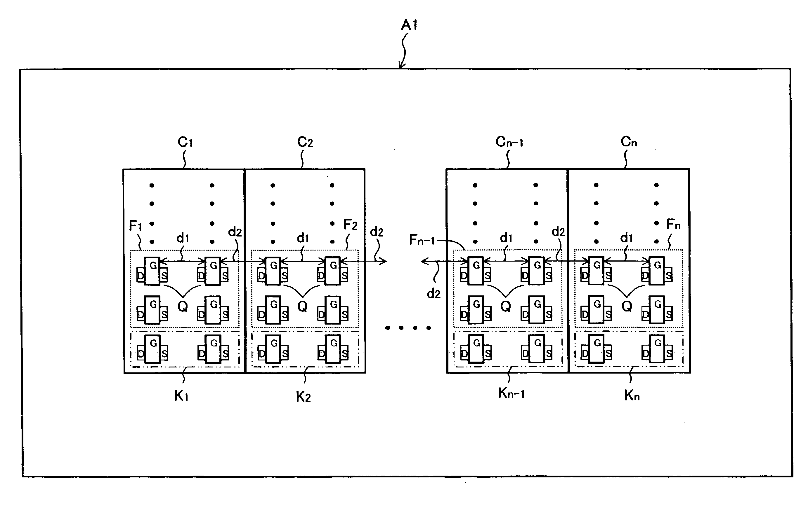
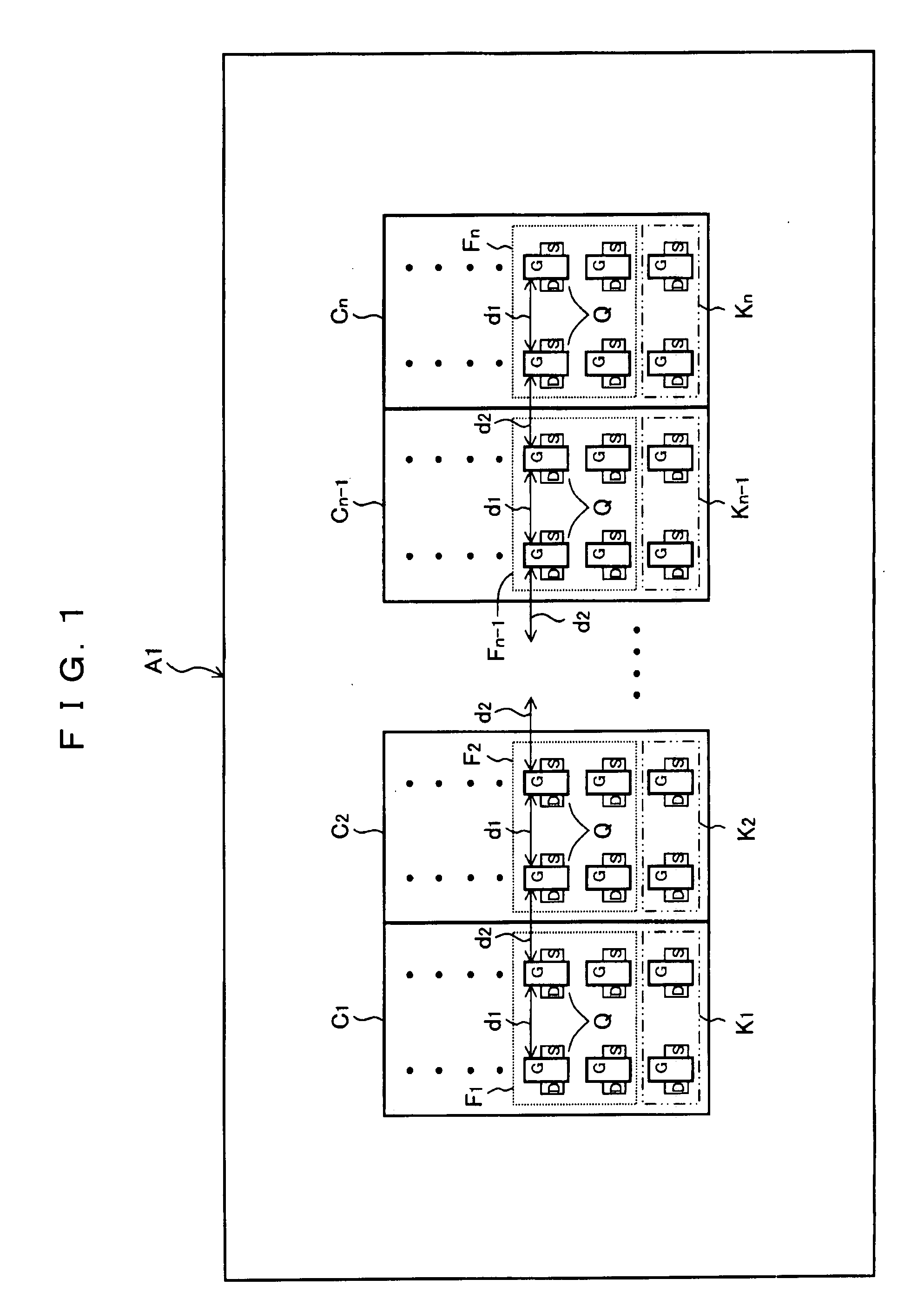
[0044]FIG. 1 is a plan view showing a schematic configuration of a semiconductor device A1 according to the first embodiment of the present invention. In FIG. 1, reference numerals C1 to Cn (where n is a natural number of two or more) are cells with the same specification in each other, and reference numerals F1 to Fn are differential amplifier circuits constituting the cell, and reference numerals K1 to Kn are current mirror circuits constituting the cell. Both of the differential amplifier circuit and the current mirror circuit are configured from a transistor pair consisting of a couple of transistor. Reference numeral d1 is a distance between one of transistor and the other of transistor in the transistor pair (It is strictly distance from the gate edge to the gate edge, and, hereafter, it is called “intra-cell distance”).

[0045]The plural cell C1 to Cn is aligned at equal intervals so as to constitute the cell group, a distance (hereafter, it is called “inter-cell distance”) d2 ...

second embodiment

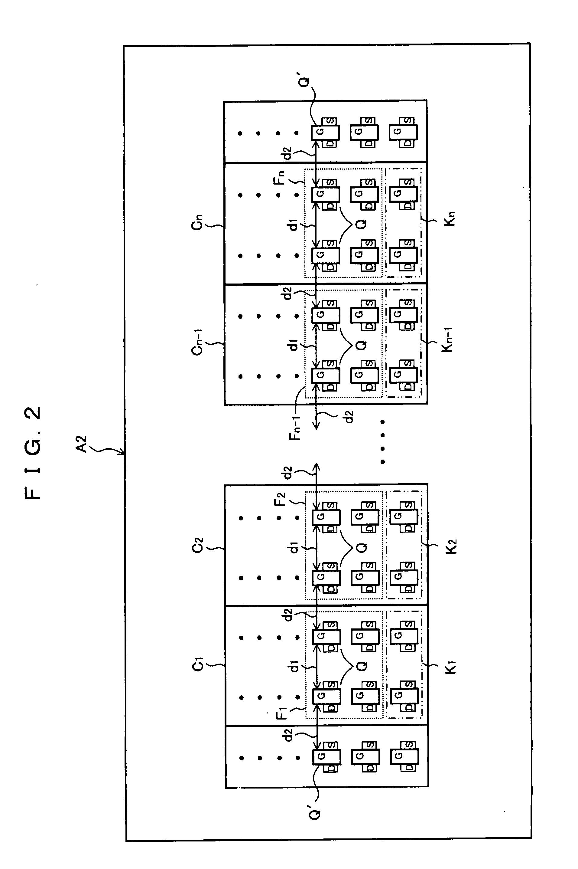
[0055]FIG. 2 is a plan view showing a schematic configuration of a semiconductor device A2 according to the second embodiment of the present invention. The same reference numeral in FIG. 1 of the first embodiment indicates the same component in FIG. 2. In this embodiment, a dummy transistor Q′ is arranged outside of the cell array direction of cells C1 and Cn in both ends of the cell group respectively, in addition to configuration of FIG. 1. The dummy transistor Q′ is arranged at a position separated by the intra-cell distance d1 from transistor Q of group end cell C1 and Cn located on the edge of the cell group. That is, the inter-cell distance d2 is equalized also here to the intra-cell distance d1 (d1=d2). The explanation is omitted about the other configuration since it is similar to the first embodiment.

[0056]According to this embodiment, since the distribution density of the transistor becomes uniform over the total length of the cell group, the relative configuration accurac...

third embodiment

[0057]FIG. 3 is a plan view showing a schematic configuration of a semiconductor device A3 according to the third embodiment of the present invention. The same reference numeral in FIG. 1 of the first embodiment indicates the same component in FIG. 3. In this embodiment, a dummy cell C′ is arranged outside of the cell array direction of cells C1 and Cn located on the edge of the cell group (both ends) respectively, in addition to the configuration of FIG. 1. The dummy cell C′ has the size and the element interval with the same specifications in each cell. The inner transistor in the dummy cell C′ is arranged at a position separated by the intra-cell distance from the transistor Q of each cell C1 and Cn located on the edge of the cell group. That is, the inter-cell distance d2 is equalized also here to the intra-cell distance d1 (d1=d2). The explanation is omitted about the other configuration since it is similar to the first embodiment.

[0058]According to this embodiment, since the d...


PUM


Abstract

The present invention is provided with a plural cell including a transistor pair. The plural cells are arranged at equal intervals so as to configure a cell group. A inter-cell distance between a transistor in one of the cell and a transistor the other cell in each of adjacent cells in the cell group is equal to a intra-cell distance between one of the transistor and the other transistor in the transistor pair.

Description

BACKGROUND OF THE INVENTION[0001]1. Field of the Invention[0002]The present invention relates to a semiconductor device provided with a plural cell including a transistor pair and having a plural output terminal and a layout method of a circuit element. In particular, the present invention relates to a liquid crystal display driver.[0003]2. Description of Related Art[0004]Conventionally, as shown in a Japanese publication patent document (Japanese Patent Application Laid-open No. 2006-101108) and a Japanese patent document (Japanese patent No. 3179424), in the semiconductor device that has a plural cell of the same specification wherein the relative configuration accuracy is requested between adjacent cells, the technique for improving an output characteristic of a plural terminal by taking matching of an element is known.[0005]For example, as for a semiconductor device that configures a liquid crystal driver, each cell is configured with an operational amplifier. An irregular lumin...

Claims


Application Information

Patent Timeline
IPC IPC(8): G06F17/50
CPCG06F17/5072G06F30/392
Inventor KOJIMA, TOMOKAZUOGAWA, MUNEHIKO
Owner PANASONIC CORP
Why Eureka
Try Eureka