Electronic component and method for manufacturing same

a technology of electronic components and manufacturing methods, applied in the direction of resistive material coating, inductance, solid-state devices, etc., can solve the problems of easy deformation of filter characteristics, easy deformation of frequency selectivity of lc filters after long-term use, etc., to achieve good efficiency, excel in heat resistance, and low cost

Active Publication Date: 2008-01-31
TDK CORPARATION
View PDF8 Cites 26 Cited by
  • Summary
  • Abstract
  • Description
  • Claims
  • Application Information

AI Technical Summary

Benefits of technology

[0016]Using a photosensitive resin layer makes it possible to form a fine and highly accurate organic insulating layer with good efficiency at a low cost. Furthermore, an organic insulating layer that excels in heat resistance is formed by heating the patterned photosensitive resin layer.
[0017]Here, the lower conductor layer typically comprises a metal such as copper, and when a lower conductor layer comprising a metal is in contact with an organic insulating layer, if the lower conductor layer is exposed to a high temperature when the photosensitive resin layer is heated, the surface of the portion that is in contact with the organic insulating layer is sometimes significantly roughened. Roughening of the lower conductor layer surface tends to increase current loss. In the case of electronic components for high-frequency applications, an electric current flows easily in the surface portion of the conductor layer due to the so-called skin effect. Therefore, the effect of surface roughening on current loss increases.
[0018]By contrast, the inventors found that roughening of the lower conductor layer surface can be effectively inhibited by heating the photosensitive resin layer in coated by the inorganic dielectric film. Further, in the electronic component obtained, a state is assumed in which the lower conductor layer surface is uniformly covered with the inorganic dielectric layer. Therefore, surface roughness of the lower conductor layer is made more uniform and the fluctuation of surface roughness within one electronic component and between a plurality of electronic components can be inhibited.
[0019]The lower conductor layer preferably includes a copper plated layer formed by plating. In the case of a copper plated layer, increase in surface roughness easily occurs due to by electromigration and heating, and the application of the present invention is especially useful.

Problems solved by technology

However, the inventors found that in the case where an organic insulating layer is in contact with a conductor layer such as a capacitor electrode portion in an electronic component of an LC composite type that has a capacitor and an inductor, when the electronic component is used as an LC filter, the filter characteristics tend to degrade easily.
More specifically, for example, frequency selectivity of the LC filter after long-term use tends to decrease easily.

Method used


Image

  • Electronic component and method for manufacturing same
  • Electronic component and method for manufacturing same
  • Electronic component and method for manufacturing same

Examples


Embodiment Construction

[0032]The preferred embodiments of the present invention will be described below in greater detail. However, the present invention is not limited to the below-described embodiments. Identical or equivalent components in the figures are in principle denoted with identical symbols.

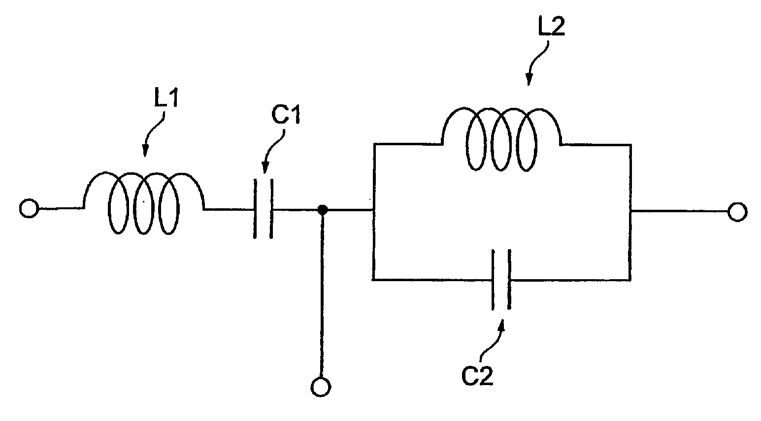
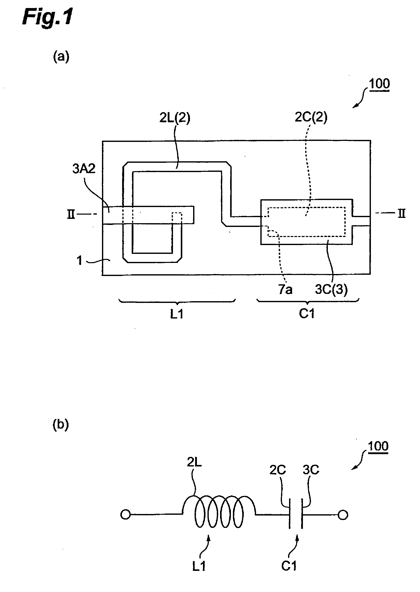
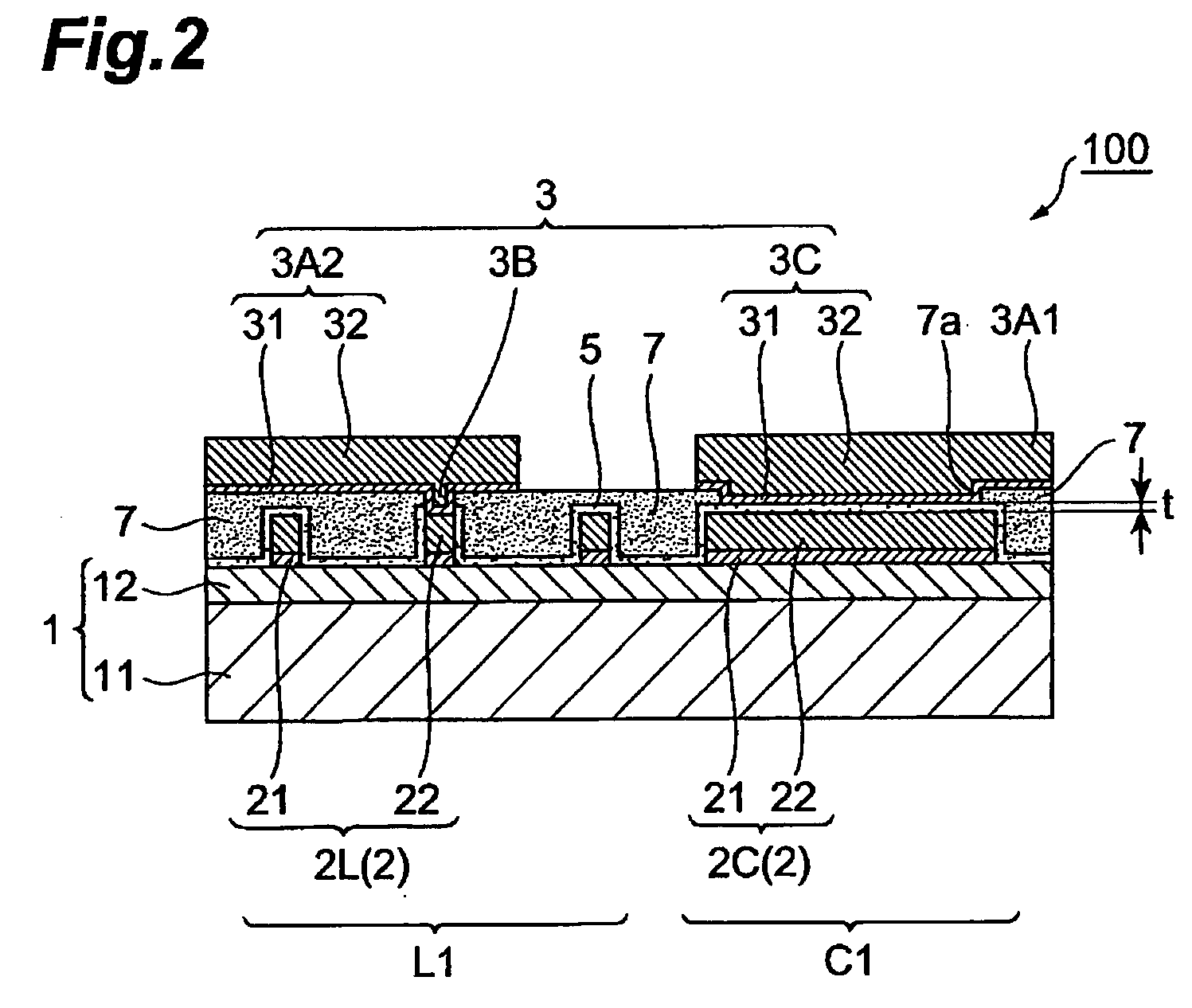
[0033]FIG. 1 is a plan view and an equivalent circuit diagram illustrating an embodiment of the electronic component in accordance with the present invention. FIG. 2 is an end view along the II-II line in (a) of FIG. 1.

[0034]An electronic component 100 shown in FIGS. 1, 2 comprises a substrate 1, a lower conductor layer 2 provided on the main surface of the substrate 1 adjacently to the substrate 1, an inorganic dielectric film 5 that covers the lower conductor layer 2, an organic insulating layer 7 provided on a surface of the inorganic dielectric film 5 on a side opposite to the substrate 1 and patterned to form an opening 7a having the inorganic dielectric film 5 as a bottom, and an upper conductor layer ...


PUM

PropertyMeasurementUnit
thicknessaaaaaaaaaa
thicknessaaaaaaaaaa
thicknessaaaaaaaaaa

Abstract

An electronic component having: a substrate, a lower conductor layer provided on the substrate; an inorganic dielectric film that covers the lower conductor layer; and an upper conductor layer having an upper electrode portion provided on the inorganic dielectric film. The lower conductor layer has a lower electrode portion that together with the upper electrode portion and the inorganic dielectric film constitutes a capacitor, and a coil portion that constitutes an inductor. The entire inorganic dielectric film is formed integrally, and the lower conductor layer is in contact only with the substrate, inorganic dielectric film, and upper conductor layer.

Description

BACKGROUND OF THE INVENTION[0001]1. Field of the Invention[0002]The present invention relates to an electronic component having an LC circuit and to a method for manufacturing the electronic component.[0003]2. Related Background Art[0004]Thin-film electronic components manufactured by using thin film formation technology are used in electronic devices such as personal computers and cellular phones. Electronic components of an LC composite type having formed therein an LC circuit having a capacitor and an inductor is one of such thin-film electronic components. Electronic components of an LC composite type are used, for example, as low pass filters, high pass filters, band pass filters, trap filters that remove signals within a predetermined frequency range, or other LC filters.[0005]A thin-film capacitor element in which a lower electrode, a dielectric layer, and an upper electrode are stacked in the order of description on a substrate has been suggested, this capacitor element havi...

Claims


Application Information

Patent Timeline
Patent Type & Authority Applications(United States)
IPC IPC(8): H01L27/01H05K1/16
CPCH01L27/016H01L28/10H01L28/40H05K1/162H05K1/165H05K2201/1006H05K2201/0175H05K2201/0179H05K2201/0195H05K2201/09509H05K3/0023
Inventor YOSHIZAWA, TOSHIYUKIMIYAZAKI, MASAHIROFURUYA, AKIRAISHIKURA, MASAOMIKUWAJIMA, HAJIME
Owner TDK CORPARATION
Why Eureka
Try Eureka