Image pickup device and method of manufacturing the same

a pickup device and image technology, applied in the direction of radio frequency controlled devices, semiconductor devices, electrical apparatus, etc., can solve the problems of difficult electrode formation and electrical connection of electrodes with external substrates, and achieve the effect of improving the yield of the image pickup devi

Active Publication Date: 2008-01-31
SAMSUNG ELECTRONICS CO LTD
View PDF21 Cites 19 Cited by
  • Summary
  • Abstract
  • Description
  • Claims
  • Application Information

AI Technical Summary

Benefits of technology

[0016]The present invention provides an image pickup device and package which can provide a high optical sensitivity and photoelectric efficiency irrespective of the structure of the wiring layers.
[0017]Another aspect of exemplary embodiments of the present invention provides an image pickup device and package which can achieve a wafer level package (WLP), simplify the manufacture process and remarkably reduce an installation space.
[0019]A related art support substrate serves merely to support the silicon substrate whereas the inventive support substrate serves to support the sensor substrate and includes contact electrodes buried therein for electrically interconnecting the wiring layers and an external substrate. The contact electrodes are formed in via holes of the support substrate and functions to interconnect the top surface side and the bottom surface side of the support substrate. The use of the contact electrodes enables modularization of the image pickup device by means of a surface mount technology (SMT), reduction of the manufacturing cost of the module, and improvement of the module performance.
[0021]The image pickup device can be manufactured by attaching a support substrate having contact electrodes buried within the support substrate on a bottom surface of the interlayer insulating film layer to be opposite to the sensor substrate; and forming a lens layer having a plurality of microlenses formed within the lens layer over the top surface of the sensor substrate to be opposite to the interlayer insulating film layer. The support substrate includes contact electrodes buried in the support substrate for interconnecting the top surface side and the bottom surface side of the support substrate, and can interconnect the wiring layers and the contact electrodes simultaneously through a process of attaching the support substrate to the interlayer insulating film layer. Accordingly, related art wires are not necessary and the image pickup device can be simply and easily mounted on the semiconductor substrate.
[0023]According to another aspect of exemplary embodiments of the present invention, there is provided a light-transmitting member which may be formed over the lens layer after formation of the lens layer. The light-transmitting member includes a light-transmitting layer covered over the lens layer and spacers for allowing the light-transmitting layer to be mounted over the sensor substrate. Also, the light-transmitting member can protect the lens layer in a state where the lens layer is opened or closed. A glass material and the like may be used for the light-transmitting layer. When the spacers hermetically seal the lens layer against the outside, they can perform an anti-dust function, thereby improving the yield of the image pickup device.

Problems solved by technology

Nevertheless, the back-illuminated image pickup device still has a shortcoming in that it is difficult to form electrodes and electrically connect the electrodes with an external substrate.
The related art image pickup device has a disadvantage in that the electrode pads can be electrically connected to the substrate via the wires, but a larger installation space in addition to the image pickup region must be secured so as to form the electrode pads as shown in FIG. 1.

Method used


Image

  • Image pickup device and method of manufacturing the same
  • Image pickup device and method of manufacturing the same
  • Image pickup device and method of manufacturing the same

Examples


Embodiment Construction

[0031]Reference will now be made in detail to exemplary embodiments of the present invention, examples of which are illustrated in the accompanying drawings, wherein like reference numerals refer to the like elements throughout. The exemplary embodiments are described below in order to explain the present invention by referring to the figures.

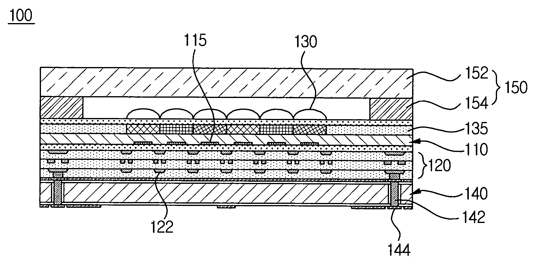
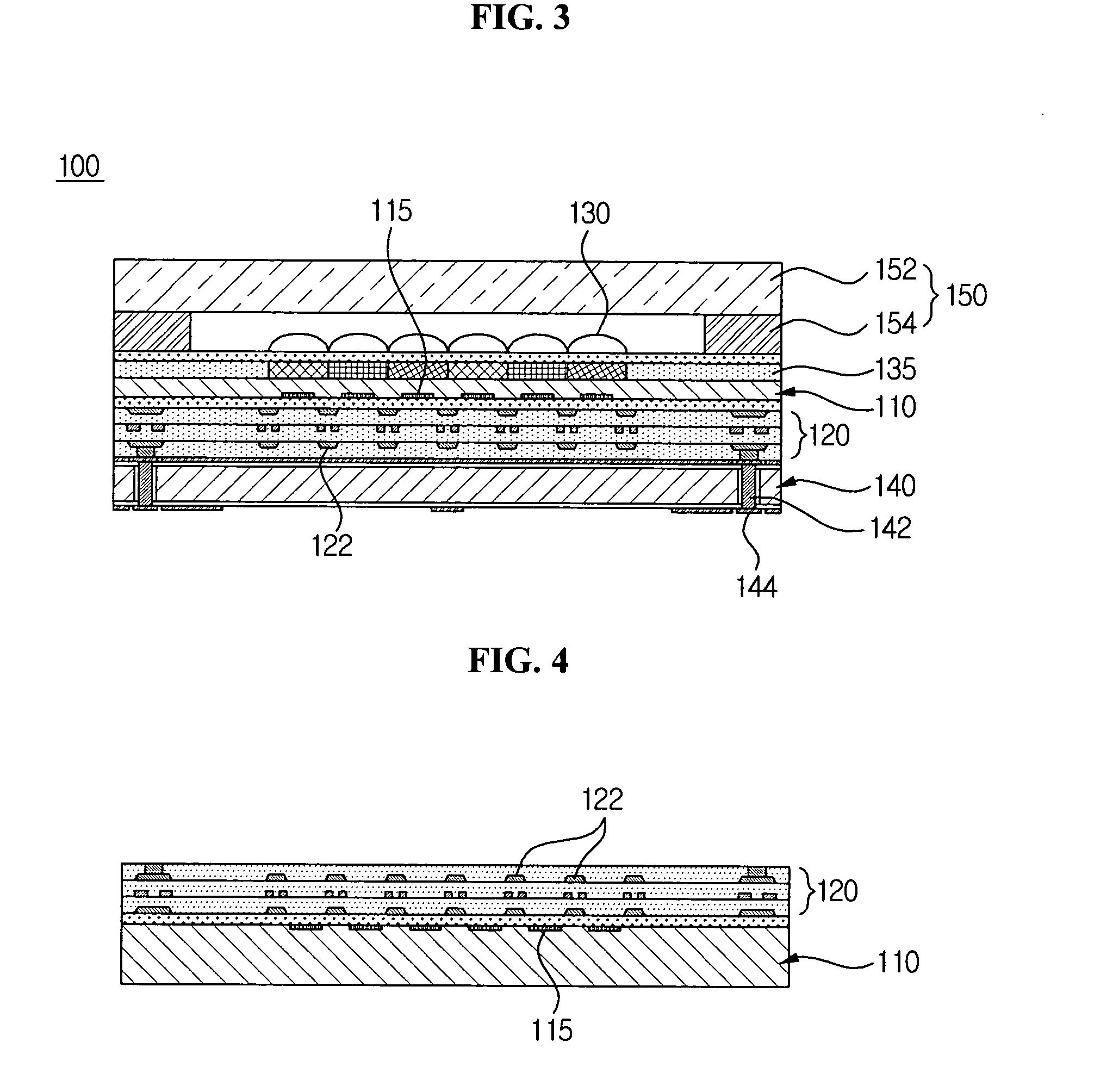
[0032]FIG. 3 is a cross-sectional view illustrating an image pickup device 100 according to an exemplary embodiment of the present invention.

[0033]Referring to FIG. 3, the image pickup device 100 includes a sensor substrate 110, an interlayer insulating film layer 120 having a plurality of insulating layers, a support substrate 140, a lens layer 130 having a plurality of microlenses formed therein, and a light-transmitting member 150.

[0034]The sensor substrate 110 has a plurality of image sensors 115 arranged in an image pickup region on the sensor substrate 110 in the form of a matrix for picking up images. Information acquired through the ima...


PUM


Abstract

An image pickup device comprises: a sensor substrate having image sensors arranged in its image pickup region in the form of a matrix; an interlayer insulating film layer formed below a bottom of the sensor substrate, the interlayer insulating film layer including wiring layers formed therein to construct an electric circuit, the wiring layer being electrically connected with the image sensors; a support substrate attached on a bottom of the interlayer insulating film layer, the support substrate having contact electrodes formed in via holes; a lens layer formed over the top surface of the sensor substrate to be opposite to the interlayer insulating film layer; and a light-transmitting member formed over the lens layer.

Description

CROSS-REFERENCE TO RELATED APPLICATION[0001]This application claims priority from Korean Patent Application No. 10-2006-0071327, filed on Jul. 28, 2006, in the Korean Intellectual Property Office, the disclosure of which is incorporated herein by reference.BACKGROUND OF THE INVENTION[0002]1. Field of the Invention[0003]Methods and apparatuses consistent with the present invention relate to an image pickup device, and more particularly to, an image pickup device which can improve optical efficiency and packaging convenience, and a method of manufacturing the image pickup device.[0004]2. Description of Related Art[0005]FIG. 1 is a perspective view illustrating the outer appearance of a related art image pickup device, and FIG. 2 is a cross-sectional view illustrating the image pickup device of FIG. 1. In FIGS. 1 and 2, there is shown a related art complementary metal-oxide semiconductor (CMOS) type image pickup device.[0006]Referring to FIGS. 1 and 2, the related art image pickup devi...

Claims


Application Information

Patent Timeline
Patent Type & Authority Applications(United States)
IPC IPC(8): H01L31/0232H01L21/00
CPCH01L27/14618H01L27/14625H01L2224/48091H01L2924/01077H01L2924/01078H01L2924/3025H01L2924/01079H01L2924/00014H01L27/146
Inventor JUNG, KYU DONGKIM, WOON BAECHOI, MIN SEOGLEE, SEUNG WAN
Owner SAMSUNG ELECTRONICS CO LTD
Why Eureka
Try Eureka