Digital-to-analog converter and image display device
a digital-to-analog converter and display device technology, applied in the direction of digital-analog convertors, instruments, cathode-ray tube indicators, etc., can solve the problems of increasing the cost of driving ic, difficult to dispose of select switches, and increasing etc., to achieve simple circuit structure, reduce the number of select switches, and high conversion precision
- Summary
- Abstract
- Description
- Claims
- Application Information
AI Technical Summary
Benefits of technology
Problems solved by technology
Method used
Image

Examples
first embodiment
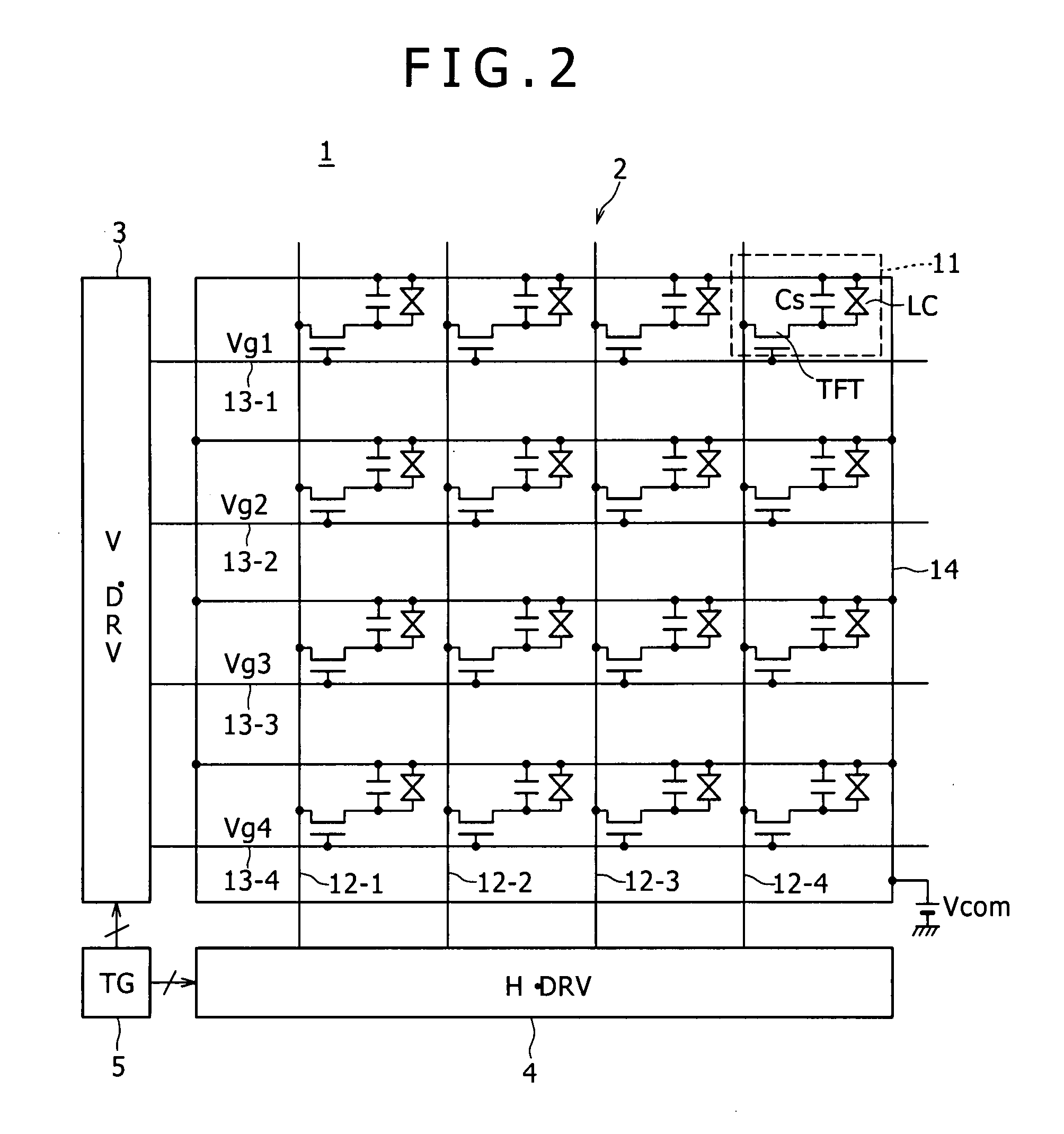
[0037]FIG. 2 is a circuit diagram showing a circuit structure of a liquid crystal display panel of an image display device according to a first embodiment of the present invention. Also, FIG. 2 shows a pixel arrangement for 4 (rows)×4 (columns) as an example for the sake of simplicity.
[0038]In a liquid crystal display panel 1 shown in FIG. 2, each of pixels 11 for 4 (rows)×4 (columns) arranged in matrix includes a thin film transistor TFT, a liquid crystal cell LC, and a holding capacitor Cs. Here, a pixel electrode of the liquid crystal cell LC is connected to one of a source and a drain of the thin film transistor TFT. Also, one electrode of the holding capacitor Cs is connected to the one of the source and the drain of the thin film transistor TFT. Signal lines (data lines) 12-1 to 12-4 are wired along a column direction of a pixel arrangement so as to correspond to columns of the pixels 11, respectively. Also, gate lines 13-1 to 13-4 are wired along a row direction of the pixel ...
second embodiment
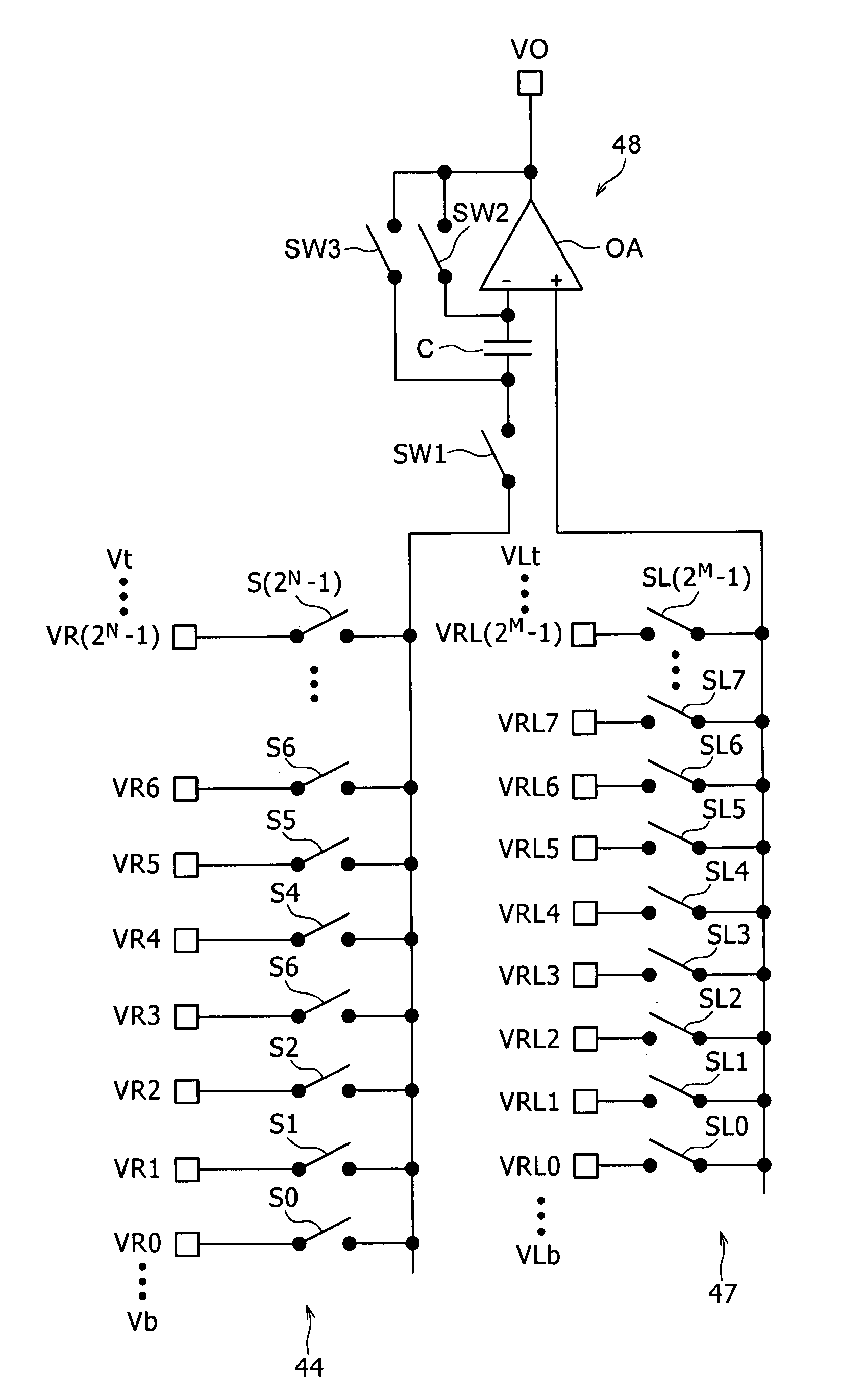
[0081]In a second embodiment of the present invention, the structure on the non-inverting input “+” side of the sample and hold amplifier 48 is improved for the purpose of realizing the higher precision D / A conversion.
[0082]In the first embodiment having the circuit structure shown in FIG. 4, the output of the lower selector 47 is directly inputted to the non-inverting input “+” of the operational amplifier OA. In this case, there is room for improvements in the following respects.
[0083]The higher capacitor C is connected to the inverting input “−” of the operational amplifier shown in FIG. 4. However, a parasitic capacitance more or less exists in the connection node between the higher capacitor C and the inverting input “−” of the operational amplifier OA. This parasitic capacitance contains a coupling capacitance between a conductive layer and another conductive layer in a semiconductor device, a junction capacitance of a semiconductor impurity region of the thin film transistor ...
third embodiment
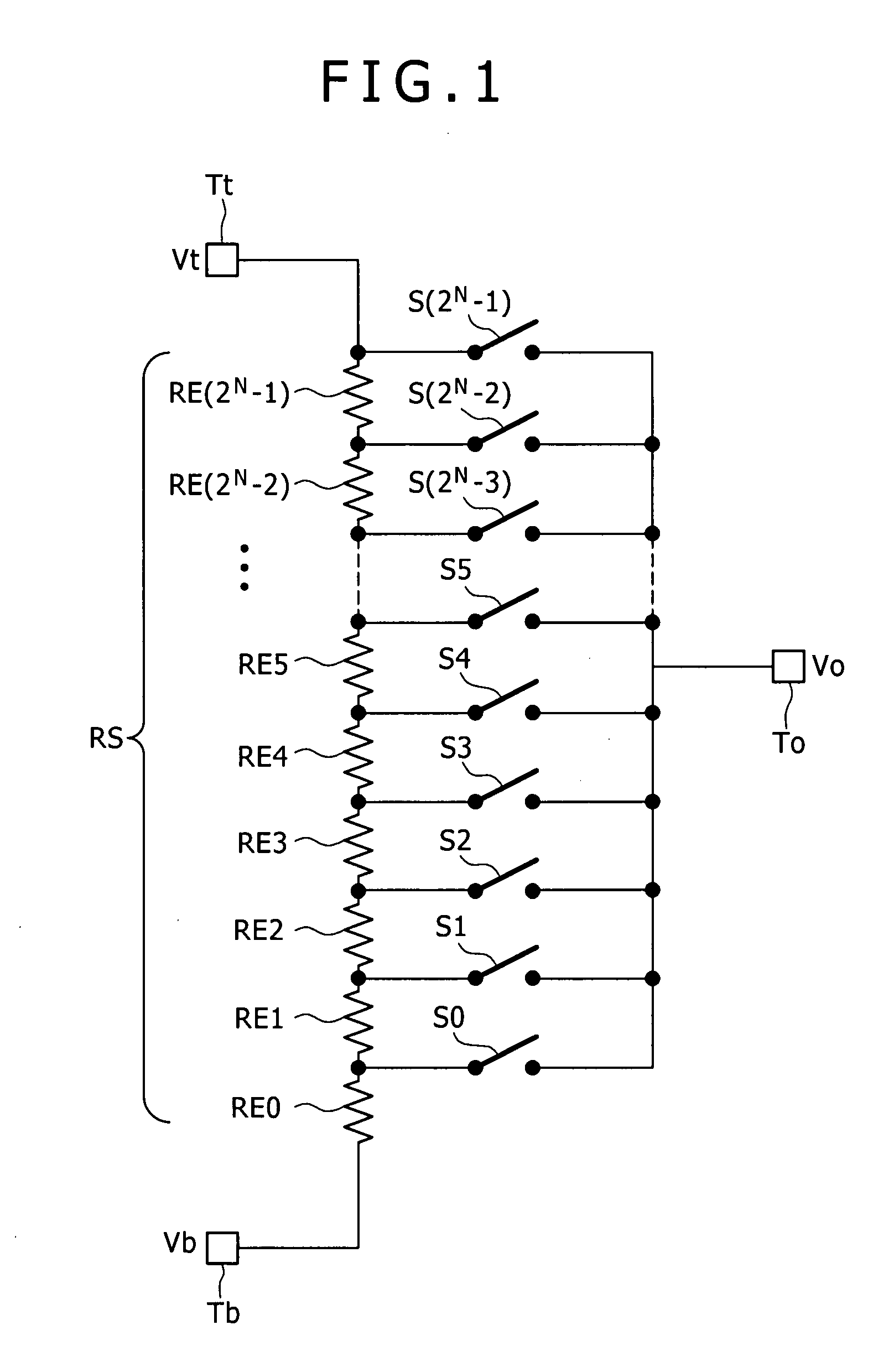
[0101]A third embodiment of the present invention relates to a resistor string, and thus can be repeatedly applied to each of the first and second embodiments of the present invention described above.
[0102]FIG. 8 shows a resistor string of a digital-to-analog converter incorporated in the image display device according to the third embodiment of the present invention.
[0103]In the block diagram of the horizontal driver 4 shown in FIG. 3, the higher resistor string 45 and the lower resistor string 46 are provided separately from each other. However, in the resistor string 50 shown in FIG. 8, the higher resistor string 45 and the lower resistor string 46 are integrated with each other so as to form a series connection body. Here, comparing the resistor string 50 of FIG. 8 with the resistor string 45 in the related art of FIG. 1, the output nodes of the higher voltage values VR0 to VR(2N−1) are shifted one resistor element to the analog lower limit Vb side. This change is also possible ...
PUM
 Abstract
Description
Claims
Application Information
 - Generate Ideas
- Intellectual Property
- Life Sciences
- Materials
- Tech Scout
- Unparalleled Data Quality
- Higher Quality Content
- 60% Fewer Hallucinations
Browse by: Latest US Patents, China's latest patents, Technical Efficacy Thesaurus, Application Domain, Technology Topic, Popular Technical Reports.
© 2025 PatSnap. All rights reserved.Legal|Privacy policy|Modern Slavery Act Transparency Statement|Sitemap|About US| Contact US: help@patsnap.com