Systems for high bandwidth one time field-programmable memory

a one-time field, programmable memory technology, applied in static storage, digital storage, instruments, etc., can solve the problems of limiting system performance, high leakage current, program disturbance, read disturbance, etc., and achieve the effect of reducing voltage levels and reducing leakage current through the array

US20080025067A1Active Publication Date: 2008-01-31SANDISK TECH LLC
87 Cites 54 Cited by

Patent Information

Authority / Receiving Office
US · United States
Patent Type
Applications(United States)
Current Assignee / Owner
Publication Date
2008-01-31

Smart Images

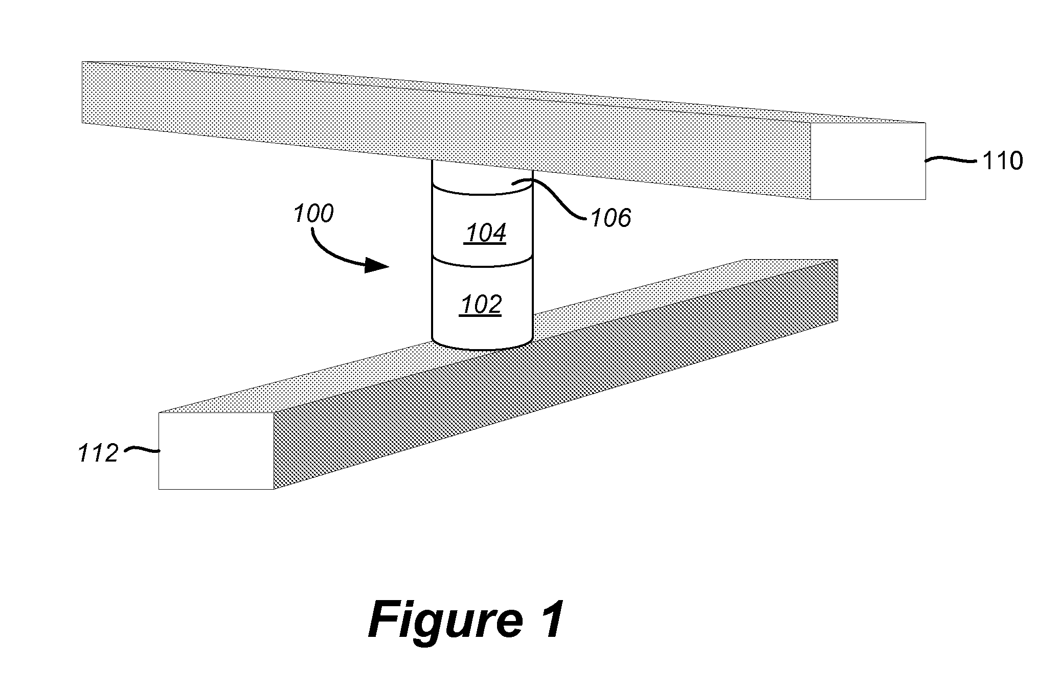
  • Figure 1
    Figure 1
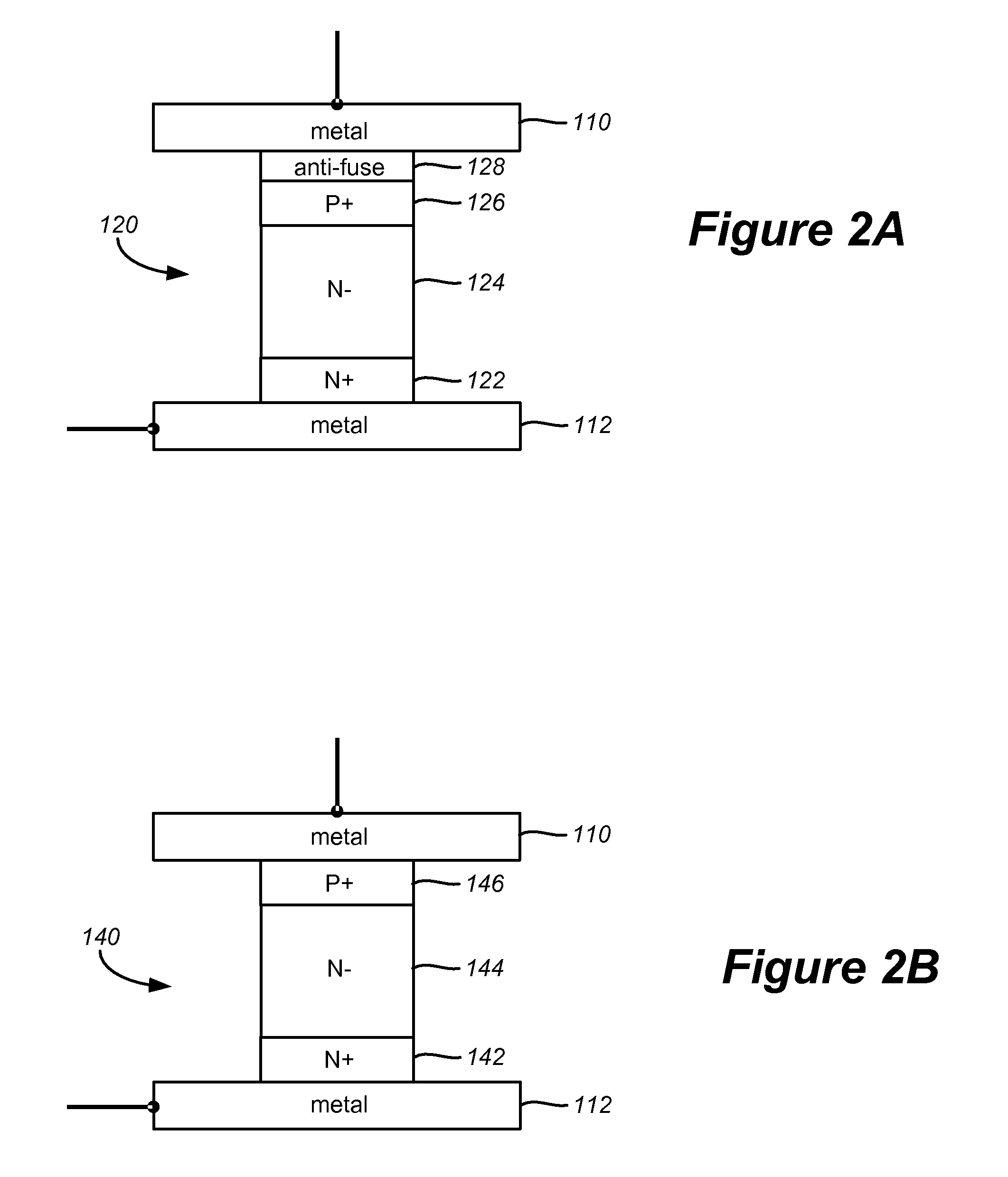
  • Figure 2
    Figure 2
  • Figure 3
    Figure 3
Patent Text Reader

Abstract

A one-time field programmable (OTP) memory cell with related manufacturing and programming techniques is disclosed. An OTP memory cell in accordance with one embodiment includes at least one resistance change element in series with a steering element. The memory cell is field programmed using a reverse bias operation that can reduce leakage currents through the array as well as decrease voltage levels that driver circuitry must normally produce in program operations. An array of memory cells can be fabricated by switching the memory cells from their initial virgin state to a second resistance state during the manufacturing process. In one embodiment, the factory switching operation can include popping an anti-fuse of each memory cell to set them into the second resistance state. The array of memory cells in the second resistance state are provided to an end-user. Control circuitry is also provided with the memory array that can switch the resistance of selected cells back toward their initial resistance state to program the array in accordance with data received from a user or host device.
Need to check novelty before this filing date? Find Prior Art

Description

CROSS-REFERENCE TO RELATED APPLICATIONS

[0001] The following related applications, filed on even date herewith, are cross-referenced and incorporated by reference herein in their entirety:

[0002] U.S. patent application Ser. No. ______ (MD-293 Attorney Docket No. SAND-01114US0), entitled “Controlled Pulse Operations in Non-Volatile Memory,” filed concurrently;

[0003] U.S. patent application Ser. No. ______ (MD-293-1 Attorney Docket No. SAND-01114US1), entitled “Systems for Controlled Pulse Operations in Non-Volatile Memory,” filed concurrently;

[0004] U.S. patent application Ser. No. ______ (MD-297 Attorney Docket No. SAND-0115US0), entitled “High Bandwidth One Time Field-Programmable Memory,” by Roy E. Scheuerlein and Christopher J. Petti;

[0005] U.S. patent application Ser. No. ______ (MD-306 Attorney Docket No. SAND-01117US0), entitled “Reverse Bias Trim Operations in Non-Volatile Memory,” by Roy E. Scheuerlein and Tanmay Kumar;

[0006] U.S. patent application Ser. No. ______ (MD-306-1 Attorn...

Examples

Embodiment Construction

[0047]FIG. 1 depicts an exemplary structure for a non-volatile memory cell that can be used in accordance with embodiments of the present disclosure. A two-terminal memory cell 100 as depicted in FIG. 1 includes a first terminal portion connected to a first conductor 110 and a second terminal portion connected to a second conductor 112. The memory cell includes a steering element 102 in series with a state change element 104 and an anti-fuse 106 to provide non-volatile date storage. The steering element can take the form of any suitable device exhibiting a nonlinear conduction current characteristic such as a simple diode. The state change element will vary by embodiment and can include numerous types of materials to store data through representative physical states. State change element 104 can include resistance change materials, phase change resistive materials, etc. For example, a semiconductor or other material having at least two levels of detectable resistance change (e.g., l...