Alignment method of a laser beam processing machine

a laser beam processing machine and alignment method technology, applied in the direction of optical radiation measurement, instruments, therapy, etc., can solve the problems of reducing the quality of each device, reducing the productivity of drilling the via hole, and unable to accurately align the alignment work of positioning the wafer on the chuck table at a predetermined location

Active Publication Date: 2008-02-07
DISCO CORP
View PDF9 Cites 33 Cited by
  • Summary
  • Abstract
  • Description
  • Claims
  • Application Information

AI Technical Summary

Benefits of technology

[0015]In the alignment method of the laser beam processing machine according to the present invention, since the insulating film formed on the processed surface of the wafer in the areas of the alignment marks is removed by picking up an image of the mark indicating crystal orientation formed at the outer periphery of the wafer held on the chuck table and bringing the design coordinate positions of the alignment marks set based on this mark indicating crystal orientation to a position right below the condenser to apply a laser beam, an image of the alignment marks can be picked up. Therefore, even a wafer having an insulating film on the processed surface held on the chuck table can be located at the predetermined position accurately.

Problems solved by technology

However, the diameters of the via holes formed in the semiconductor wafer are as small as 100 to 300 μm, and drilling the via holes is not always satisfactory in terms of productivity.
Although a conductive material such as aluminum or copper is embedded in the via holes formed in the substrate as described above, when aluminum or copper is directly embedded in the via holes, there is a problem that aluminum or copper atoms diffuse into the inside of the substrate made of silicon to reduce the quality of each device.
Therefore, there is a problem that alignment work for positioning the wafer held on the chuck table at a predetermined location accurately cannot be carried out.

Method used


Image

  • Alignment method of a laser beam processing machine
  • Alignment method of a laser beam processing machine
  • Alignment method of a laser beam processing machine

Examples


Embodiment Construction

[0032]A preferred embodiment of the present invention will be described in detail hereinbelow with reference to the accompanying drawings.

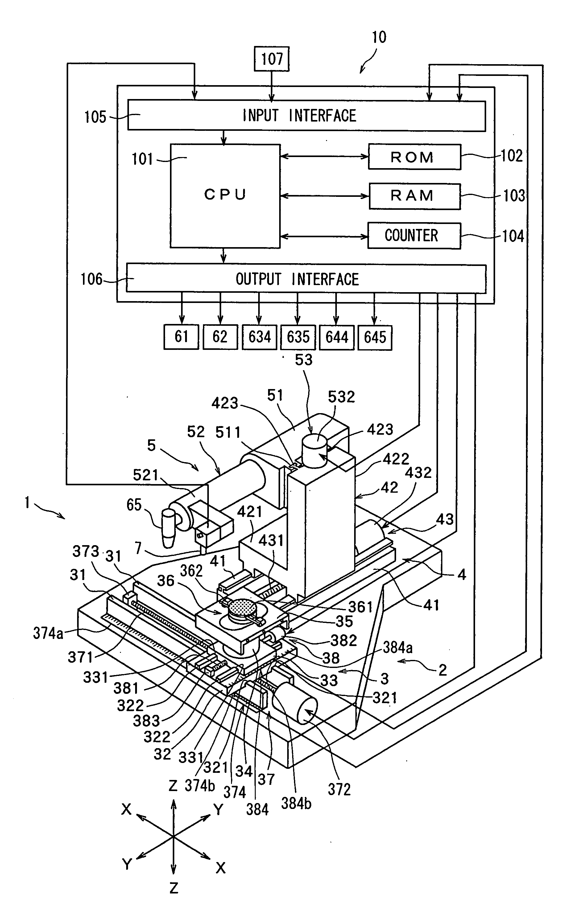
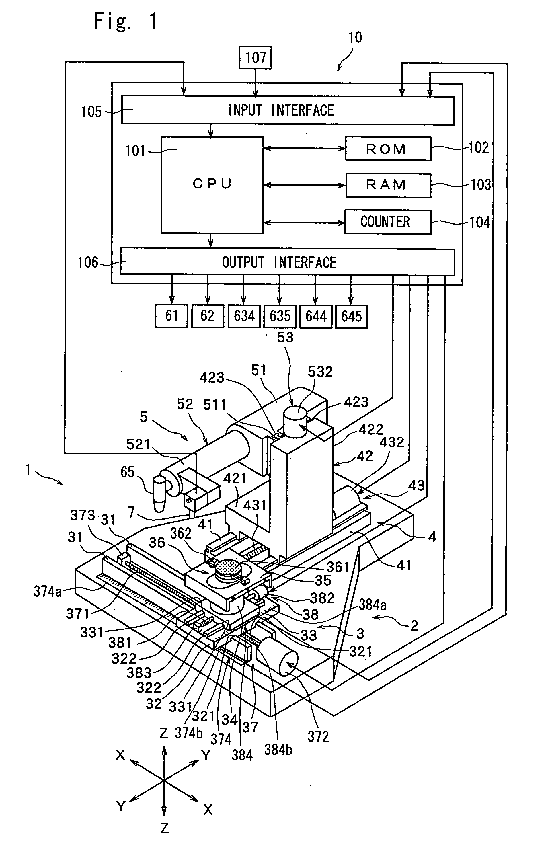
[0033]FIG. 1 is a perspective view of a laser beam processing machine for carrying out the alignment method of the present invention.

[0034]The laser beam processing machine 1 shown in FIG. 1 comprises a stationary base 2, a chuck table mechanism 3 for holding a workpiece, which is mounted on the stationary base 2 in such a manner that it can move in a processing-feed direction (X direction) indicated by an arrow X, a laser beam application unit support mechanism 4 mounted on the stationary base 2 in such a manner that it can move in an indexing-feed direction (Y direction) indicated by an arrow Y perpendicular to the direction indicated by the arrow X, and a laser beam application unit 5 mounted on the laser beam application unit support mechanism 4 in such a manner that it can move in a direction (Z direction) indicated by an arrow Z.
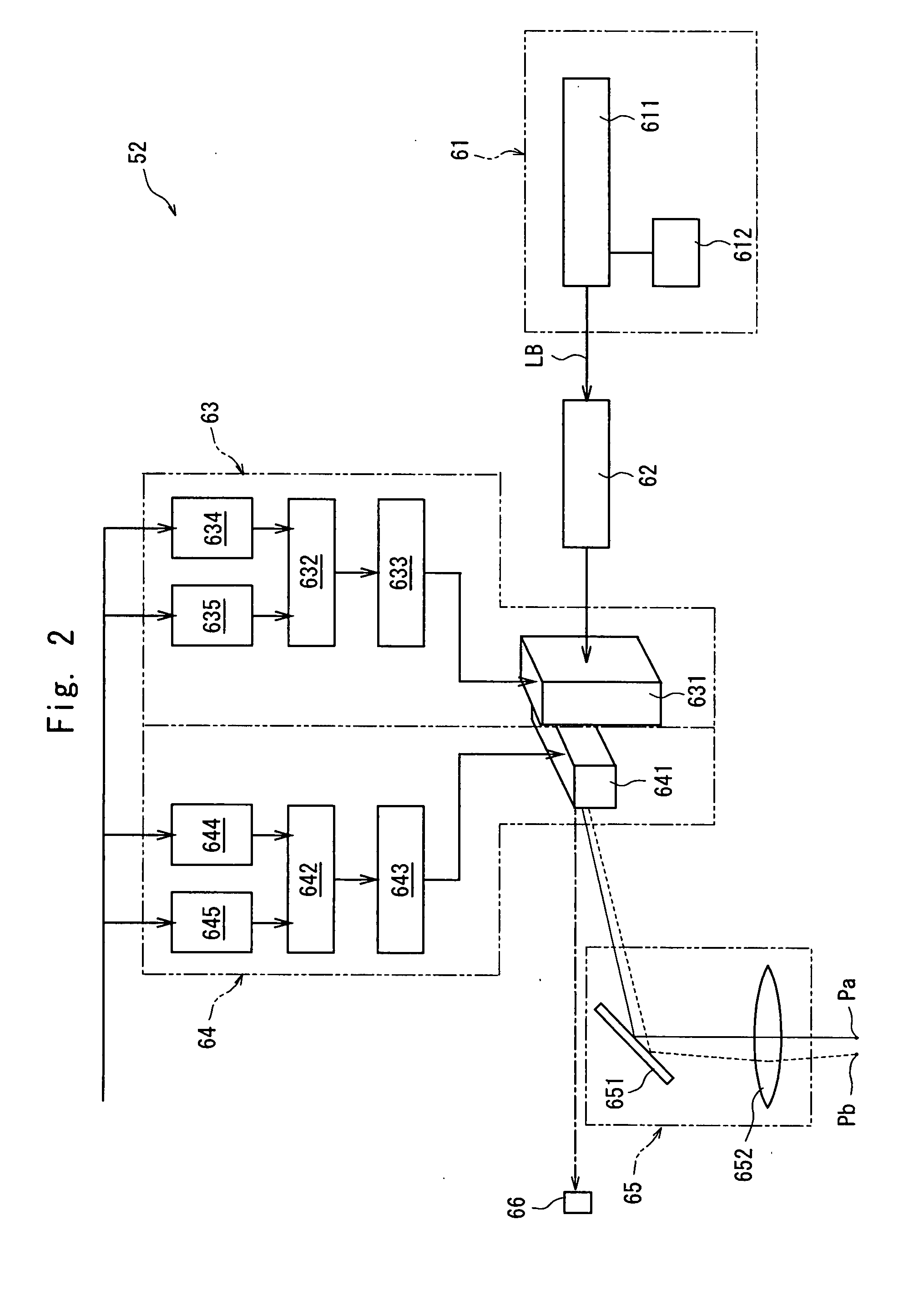
[0035]The ab...


PUM

PropertyMeasurementUnit
diametersaaaaaaaaaa
thicknessaaaaaaaaaa
wavelengthaaaaaaaaaa

Abstract

An alignment method of a laser beam processing machine comprising a chuck table, a laser beam application means having a condenser for applying a laser beam to the workpiece held on the chuck table, an image pick-up means for picking up an image of the workpiece held on the chuck table and a control means having a memory for storing the specifications of the workpiece, the method comprising the steps of storing the design coordinates of a processing position set based on the mark indicating the crystal orientation of a wafer and alignment marks; picking up an image of the periphery of the wafer with the image pick-up means and locating the mark indicating the crystal orientation of the wafer at a predetermined position; positioning the design coordinate position of each of the alignment marks set based on the mark indicating the crystal orientation of the wafer right below the condenser and applying a laser beam from the condenser so as to remove the insulating film in the alignment mark areas; and picking up an image of the alignment marks with the image pick-up means and adjusting the coordinates of the processing position of the wafer on the chuck table based on the image of the alignment marks.

Description

FIELD OF THE INVENTION[0001]The present invention relates to an alignment method of a laser beam processing machine for laser-processing a wafer having an insulating film coated on the processed surface of the substrate of a semiconductor wafer and the like.DESCRIPTION OF THE PRIOR ART[0002]In the production process of a semiconductor device, a plurality of areas are sectioned by dividing lines called “streets” arranged in a lattice pattern on the front surface of a substantially disk-like semiconductor wafer, and a device such as IC, LSI or the like is formed in each of the sectioned areas. Individual semiconductor chips are manufactured by cutting this semiconductor wafer along the streets to divide it into the areas having each a device formed therein.[0003]To reduce the size and increase the number of functions of an apparatus, a modular structure for connecting the bonding pads of laminated devices composed of a plurality of semiconductor chips is disclosed by JP-A 2003-163323....

Claims


Application Information

Patent Timeline
Patent Type & Authority Applications(United States)
IPC IPC(8): G01N23/00B23K26/02H01L21/02H01L21/68
CPCB23K26/04B23K26/045B23K26/0626B23K26/0853B23K26/043B23K26/4075B23K2201/40H01L21/67294H01L21/682B23K26/386B23K26/044B23K26/40B23K26/389B23K2101/40B23K2103/50
Inventor MORIKAZU, HIROSHIKAWAGISHI, ERI
Owner DISCO CORP
Why Eureka
Try Eureka