Line Head and Image Forming Apparatus Using the Same

a technology of image forming apparatus and line head, which is applied in the direction of electrographic process apparatus, printing, instruments, etc., can solve the problems of inability to create favorable spots, failure to form favorable spots, and inability to obtain sufficient drive current, so as to reduce the number of driver ics, reduce the probability of occurrence, and improve the effect of resolution

Inactive Publication Date: 2008-02-07
SEIKO EPSON CORP
View PDF7 Cites 31 Cited by
  • Summary
  • Abstract
  • Description
  • Claims
  • Application Information

AI Technical Summary

Benefits of technology

[0014]A second advantage of some aspects of the invention is to provide a technique which makes it possible for a line head which is capable of imaging a light beam on a surface-to-be-scanned and forming plural spots next to each other to form favorable spots while discouraging occurrence of a defect that two spots which are supposed to be contiguous to each other fail to be contiguous and become discontiguous.
[0015]In the line head described in JP-A-9-226171, the plural organic EL elements and the driver ICs are formed separated from each other on the chip-on-board substrate and the bonding wires electrically connect them with each other. This demands large mounting areas for the organic EL elements, the driver ICs, etc. This also dramatically increases the number of the organic EL elements to be mounted on the substrate in order to meet a recently required high resolution, and hence, increases the number of the driver ICs to be mounted. The mounting space to mount the driver ICs therefore becomes small, which gives rise to a problem that it is not possible to obtain a sufficient drive current to drive the organic EL elements. Further, the increased number of the organic EL elements and the driver ICs makes it difficult to ensure an interconnection space. Due to these factors, it is increasingly difficult to satisfy the needs for size reduction of the line head and a higher resolution at the same time.
[0016]A third advantage of some aspects of the invention is to provide a high-resolution compact line head and an image forming apparatus which comprises such a line head.
[0017]For the purpose of forming spots with as much light as possible, it is preferable that in the line head described above, light beams emitted the light emitting elements impinge upon the associated imaging lenses to the maximum extent. However, the following problem may occur with the farthest light emitting element (outer-most element) from the optical axis of the associated imaging lens among the light emitting elements of the light emitting element group. That is, due to an inappropriate relationship between the outer-most element and the diameter of the imaging lens corresponding to the outer-most element, of the light bean emitted from the outer-most element, the amount of the light beam which impinges upon the imaging lens decreases. This reduces the amount of the light beam which contributes to creation of a spot which corresponds to the outer-most element and may sometimes prevent favorable spot creation.
[0018]A fourth advantage of some aspects of the invention is to provide a technique which makes it possible to form an excellent spot while suppressing a decrease of the amount of the light beam which contributes to creation of a spot which corresponds to the outer-most element in a line head which images, with its imaging lenses corresponding to multiple light emitting elements, light beams emitted from the multiple light emitting elements on a surface-to-be-scanned.

Problems solved by technology

This may result in a problem that it is not possible to create a favorable spot.
However, a varied structure of the apparatus or the like may sometimes give rise to a defect that two spots intended to be contiguous to each other on a surface-to-be-scanned are isolated from each other, which is a failure of forming favorable spots.
The mounting space to mount the driver ICs therefore becomes small, which gives rise to a problem that it is not possible to obtain a sufficient drive current to drive the organic EL elements.
Further, the increased number of the organic EL elements and the driver ICs makes it difficult to ensure an interconnection space.
Due to these factors, it is increasingly difficult to satisfy the needs for size reduction of the line head and a higher resolution at the same time.
However, the following problem may occur with the farthest light emitting element (outer-most element) from the optical axis of the associated imaging lens among the light emitting elements of the light emitting element group.
That is, due to an inappropriate relationship between the outer-most element and the diameter of the imaging lens corresponding to the outer-most element, of the light bean emitted from the outer-most element, the amount of the light beam which impinges upon the imaging lens decreases.

Method used


Image

  • Line Head and Image Forming Apparatus  Using the Same
  • Line Head and Image Forming Apparatus  Using the Same
  • Line Head and Image Forming Apparatus  Using the Same

Examples


first embodiment

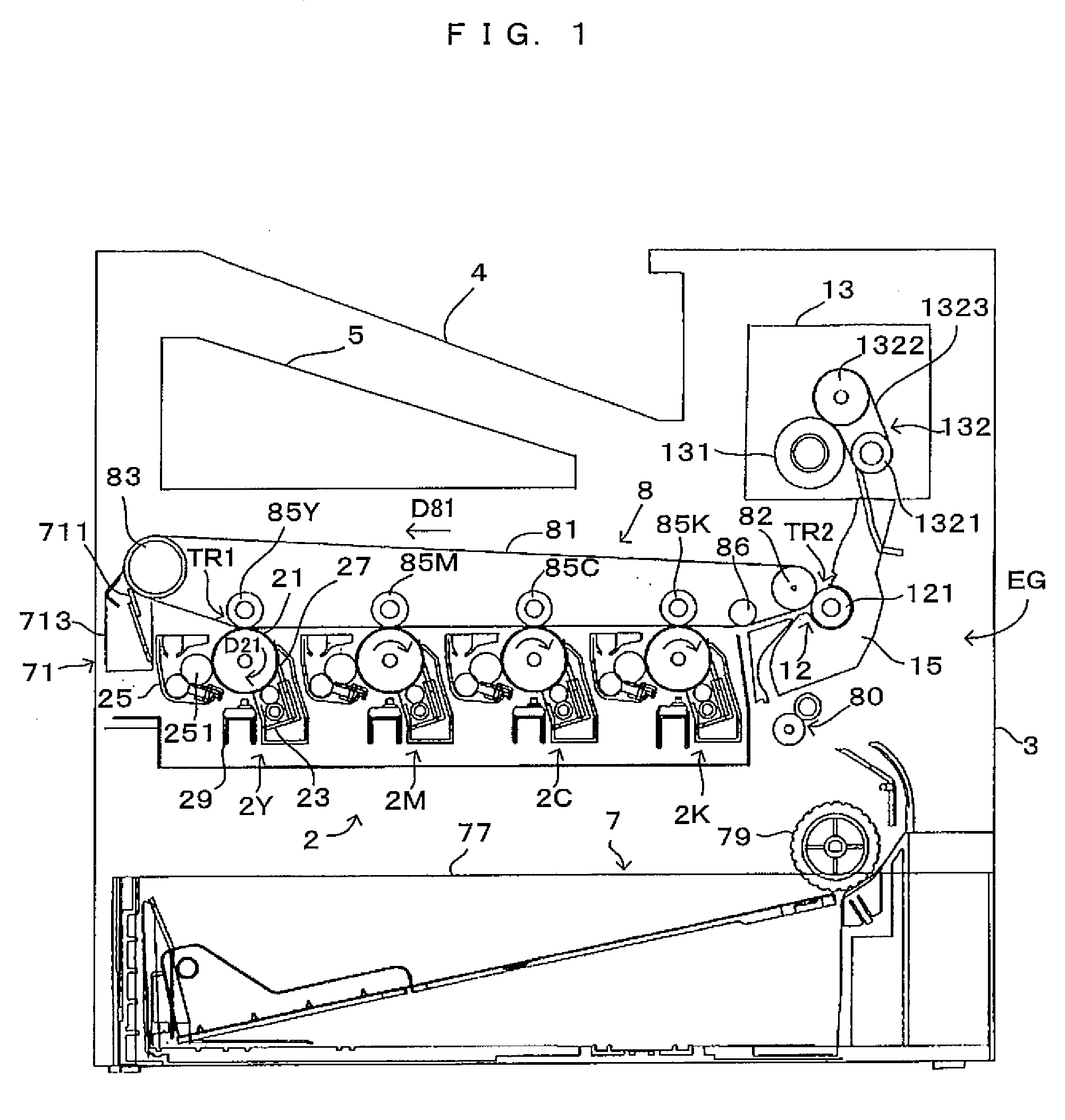
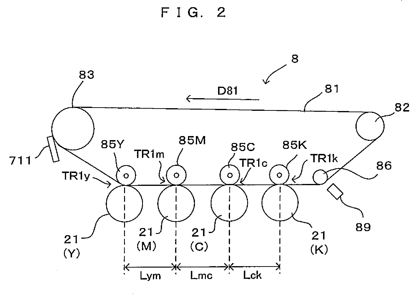
[0067]FIG. 1 is a drawing which shows an image forming apparatus according to a first embodiment of the invention. FIG. 2 is a drawing which shows an arrangement of image forming stations in the image forming apparatus of FIG. 1. FIG. 3 is a drawing which shows the electric structure of the image forming apparatus shown in FIG. 1. This apparatus is an image forming apparatus which is capable of selectively executing a color mode for superimposing toner in four colors of black (K), cyan (C), magenta (M) and yellow (Y) one atop the other and accordingly forming a color image and a monochrome mode for forming a monochrome image using toner in the black color (K) alone. In this image forming apparatus, when an external apparatus such as a host computer gives an image forming command to a main controller MC which comprises a CPU, a memory and the like, the main controller MC provides an engine controller EC with a control signal or the like. Based on the signal or the like, the engine co...

second embodiment

[0123]Although the embodiments above require forming the light emitting element groups 295 in the manner shown in FIG. 8, the structure of the light emitting element groups 295 is not limited to this. The important benefit is that as the embodiments require that the main-scanning-direction group pitch Px is wider than the sub-scanning-direction group pitch Py in the line head which has the structure that the main-scanning-direction group width Gx is wider than the sub-scanning-direction group width Gy, it is possible to form favorable spots while suppressing crosstalk in the main scanning direction MD. The light emitting element groups may therefore be formed as described below, for instance.

[0124]FIG. 16 is a drawing which shows the structure of the light emitting element groups according to a second embodiment of the invention. In FIG. 16, one light emitting element group 295 is formed by arranging in the lateral direction LTD corresponding to the sub scanning direction SD two lig...

third embodiment

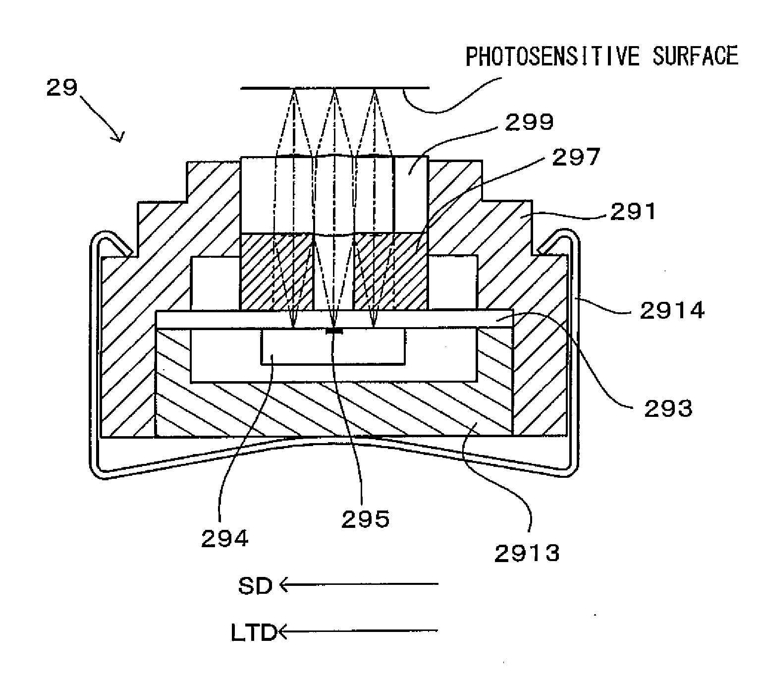
[0127]FIG. 17 is a cross sectional view of the line head (exposure section) according to a third embodiment of the invention taken along the sub scanning direction. In short, the line head shown in FIG. 17 uses LEDs as the light emitting elements. A major difference from the line head which uses organic ELs as the light emitting elements described with reference to FIG. 4 lies in the positions at which the light emitting elements are disposed. As shown in FIG. 5, in the line head which uses organic ELs as the light emitting elements, the light emitting elements (light emitting element groups 295) are disposed on the back surface of the glass substrate 293. Meanwhile, in the line head shown in FIG. 17 which uses LEDs as the light emitting elements, the light emitting elements are disposed on the front surface of the glass substrate 293. The other structures are common between the line heads shown in FIGS. 5 and 17, and therefore, the common features are denoted at corresponding refer...


PUM


Abstract

A line head includes multiple light emitting element groups each including multiple light emitting elements. In each light emitting element group, the multiple light emitting elements are disposed in a two-dimensional arrangement so that a distance Gx is greater than a distance Gy. The light emitting element groups are arranged so that pitches Px are greater than pitches Py.

Description

CROSS REFERENCE TO RELATED APPLICATION[0001]The disclosure of Japanese Patent Applications enumerated below including specification, drawings and claims is incorporated herein by reference in its entirety:[0002]No. 2006-213299 filed Aug. 4, 2006;[0003]No. 2006-213301 filed Aug. 4, 2006;[0004]No. 2006-241452 filed Sep. 6, 2006; and[0005]No. 2006-257237 filed Sep. 22, 2006.BACKGROUND[0006]1. Technical Field[0007]The present invention relates to a line head which make a light beam scan a surface-to-be-scanned and an image forming apparatus which uses the same.[0008]2. Related Art[0009]Proposed is a line head which uses a light emitting element group (i.e., “the light emitting element array” described in JP-A-2000-158705) which is formed by an arrangement of multiple light emitting elements as that according to JP-A-2000-158705. Further, in the line head, multiple light emitting element groups are arranged and one imaging lens is disposed as it is opposed to each one of the multiple lig...

Claims


Application Information

Patent Timeline
Patent Type & Authority Applications(United States)
IPC IPC(8): B41J2/385G02B27/00
CPCB41J2/45G03G15/326G03G15/04072G03G2215/0451G03G2215/0407
Inventor NOMURA, YUJIROINOUE, NOZOMUKOIZUMI, RYUTAIKUMA, KEN
Owner SEIKO EPSON CORP
Why Eureka
Try Eureka