Optical Circuit Device

a circuit device and optical circuit technology, applied in the field of optical communication, can solve the problems of polarization dependence of propagation characteristic, significant obstacle to practical application, and extremely large pdl (polarization dependent loss) of 4.5 db or more, so as to achieve the effect of reducing insertion loss and connection cost, reducing pdl, and not deteriorating the polarization extinction ratio

Inactive Publication Date: 2008-02-07
FURUKAWA ELECTRIC CO LTD
View PDF4 Cites 69 Cited by
  • Summary
  • Abstract
  • Description
  • Claims
  • Application Information

AI Technical Summary

Benefits of technology

[0031] According to the present invention, as an incoming light beam is split into two polarization beams by the polarization beam splitter/combiner, one of the polarization beam has a polarization plane rotated by the polarization rotator so as to match the polarization plane with that of the other polarization beam and input to the optical circuit, there only exists polarization beams of the same polarization plane in the optical circuit. Besides, as no PMF is used, the polarization extinction ratio is not deteriorated and the PDL can be reduced significantly. Further, as no PMF is used, there is no connection between the PMF and any other component, and therefore, the insertion loss and the connection cost can be reduced significantly and the reliability of the connection can be enhanced. Furthermore, as no PMF is used, there is no need to consider installation of the PMF, and therefore, modules of the optical circuit device can be downsized. Furthermore, as there is no expensive PMF block used, the fabrication cost of the optical circuit device can

Problems solved by technology

However, for TM (Transverse Magnetic) polarization beam, the profile was not flattened and there occurred an extremely large PDL (Polarization Dependent Loss) of 4.5 dB or more.
This PDL may be 10 dB or more depending on the wavelength characteristic of the optical amplifier, which sometimes becomes a significant o

Method used


Image

  • Optical Circuit Device
  • Optical Circuit Device
  • Optical Circuit Device

Examples


first embodiment

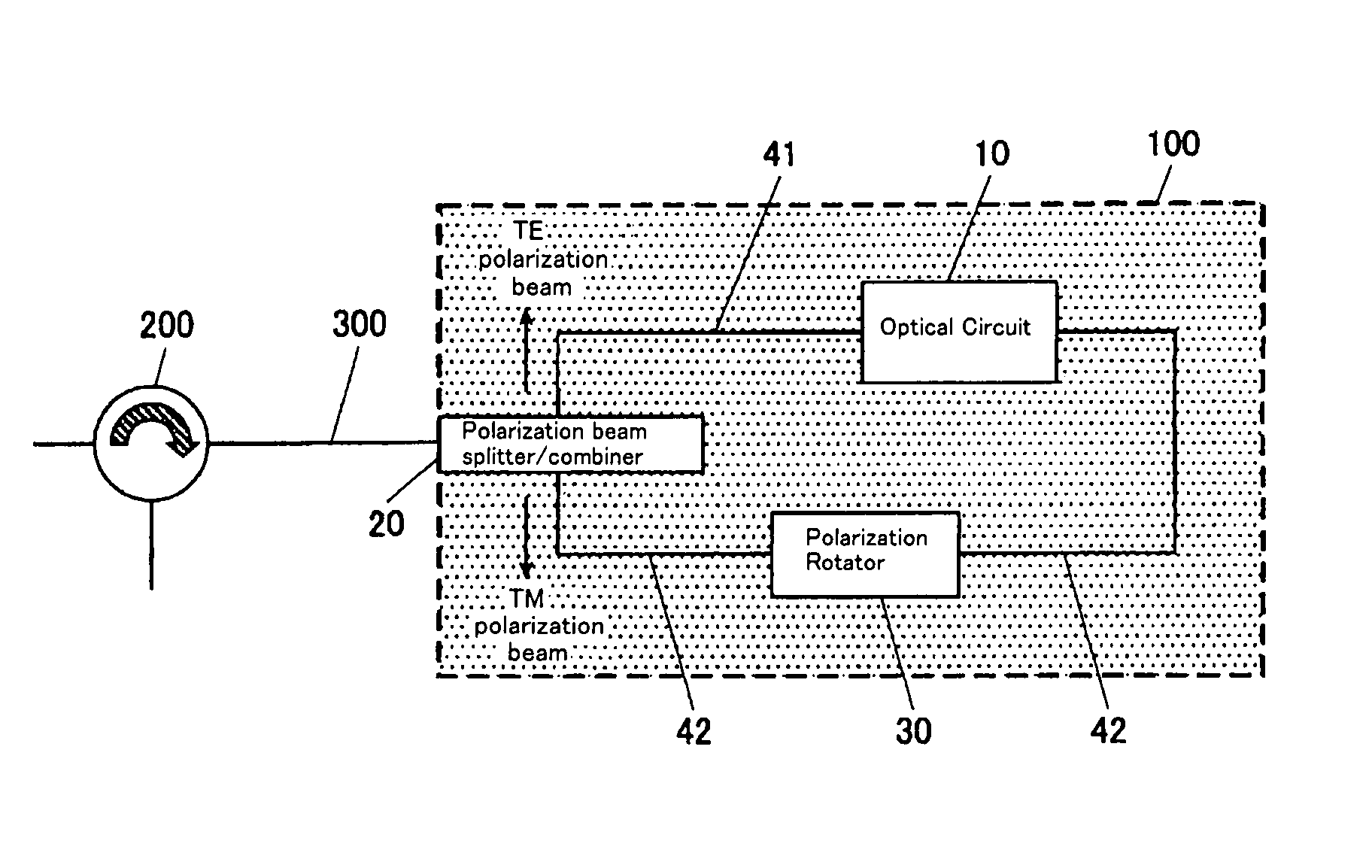
[0093] The first embodiment of the present invention is described with reference to FIG. 1. First explanation is made about a configuration of an optical circuit device 100 of the present embodiment referring to FIG. 1. FIG. 1 illustrates the configuration of the optical circuit device 100.

[0094] As illustrated in FIG. 1, the optical circuit device 100 is a PLC and includes on a planar substrate, an optical circuit 10i a polarization beam splitter / combiner 20, a polarization rotator 30, optical waveguides 41 and 42, which are all monolithically integrated in one chip. The polarization beam splitter / combiner 20 formed on the optical circuit device 100 is connected to a circulator 200 via a SMF 300.

[0095] The polarization beam splitter / combiner 20 is connected to the optical circuit 10 via the two paths of the optical waveguides 41 and 42. Besides, the polarization rotator 30 is provided on the optical waveguide 42.

[0096] The optical circuit 10 is, for example, a dynamic gain equal...

second embodiment

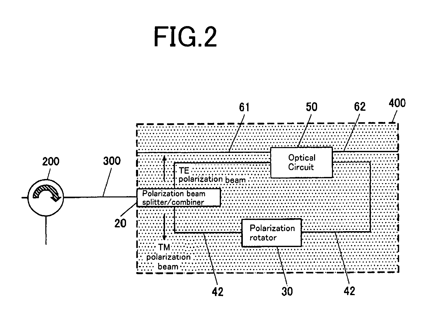
[0102] Next description is made about a second embodiment of the present invention with reference to FIG. 2. First, the configuration of an optical circuit device 400 of this embodiment is described with reference to FIG. 2. FIG. 2 illustrates the optical circuit device 400 of this embodiment.

[0103] As illustrated in FIG. 2, the optical circuit device 400 of this embodiment is a PLC and has an optical circuit 50, a polarization beam splitter / combiner 20, a polarization rotator 30, optical waveguides 41 and 42, a monitor input waveguide 61 and a monitor output waveguide62, which are all monolithically integrated in one chip. In other words, the optical circuit device 400 is configured by adding the monitor input waveguide 61 and the monitor output waveguide 62 to the optical circuit device 100 of the first embodiment. In the description below, portions having the same functions as those illustrated in the above-described figure are indicated by the same numerals and description ther...

example 1

[0107] With reference to FIGS. 3 and 4, described as a specific example 1 of the above-described embodiment 1 is a configuration in which a dynamic gain equalizer having characteristic adjusting function by use of the thermo-optic effect is applied the optical circuit 10 of the optical circuit device 100 in FIG. 1. FIG. 3 illustrates the configuration of an optical circuit device 100A of this example.

[0108] As illustrated in FIG. 3, the integrated PLC-type optical circuit device 100A of this example is configured to include in the optical circuit device 100 of FIG. 1, a dynamic gain equalizer 10A as the optical circuit 10, a polarization beam splitter / combiner 20A as the polarization beam splitter / combiner 20 and a half wave plate 30A as the polarization rotator 30.

[0109] The polarization beam splitter / combiner 20A has optical couplers 21 as optical circuits having the polarization beam splitting and combining function cascaded at two stages in the same substrate. Besides, used as...


PUM


Abstract

The present invention provide an optical circuit device having: an optical circuit; a polarization beam splitter/combiner for splitting an incoming light beam into two polarization beams and combining the two polarization beams into an outgoing light beam; a first optical waveguide and a second optical waveguide for connecting the optical circuit and the polarization beam splitter/combiner and receiving the two polarization beams independently; and a polarization rotator, arranged on the first optical waveguide, for rotating a polarization plane of one of the two polarization beams split by the polarization beam splitter/combiner so as to match a polarization plane of the other of the two polarization beams, the optical circuit, the polarization beam splitter/combiner, the first optical waveguide, the second optical waveguide and the polarization rotator being integrated on a planar substrate.

Description

TECHNICAL FIELD [0001] The present invention relates to an optical communication field. BACKGROUND ART [0002] Conventionally, among optical components used in a DWDM (Dense Wavelength Division Multiplexing) system an optical component using a planar lightwave circuit (PLC) comes into practical use in a splitter or the like and is regarded as an up-and-coming device in view of high controllability and stability. With an eye toward development of the DWDM system in future, optical circuits using a PLC to serve as a dynamic gain equalizer, a tunable dispersion compensator and the like have been already developed. [0003] Generally used to exhibit variable characteristics in these optical circuits is the thermo-optic effect. The thermo-optic effect is such a phenomenon that the refractive index of a silica glass or the like varies depending on the temperature. When the refractive index of an optical waveguide is changed with the thermo-optic effect, the effective refractive index of the ...

Claims


Application Information

Patent Timeline
IPC IPC(8): G02B6/12
CPCG02B6/12007G02B6/12019G02B6/29352G02B6/274G02B6/2793G02B6/126
Inventor MATSUBARA, NORITAKAKAWASHIMA, HIROSHINARA, KAZUTAKA
Owner FURUKAWA ELECTRIC CO LTD
Why Eureka
Try Eureka