Semiconductor structures including vertical diode structures and methods of making the same

Inactive Publication Date: 2008-02-07
MICRON TECH INC
View PDF51 Cites 11 Cited by
  • Summary
  • Abstract
  • Description
  • Claims
  • Application Information

AI Technical Summary

Benefits of technology

[0023] Since the diode has a vertical formation, use of the surface area on the silicon microchip is minimized. Furthermore, as there is only one connection point on top of the diode, the diode is easier to connect to other elements and is easier to size.
[0024] In one alternative embodiment, a programmable resistor is positioned between the metal contact and the top portion of the silicon plug. The programmable resistor comprises chalcogenide material and barrier mater

Problems solved by technology

This movement has increased the number and complexity of circuits on a single microchip.
An ideal diode will allow an electrical current to flow through the diode in one direction but will not allow an electrical current to flow through the diode in the opposite direction.
This side-by-side positioning, however, uses a relatively large amount of surface space on the microchip.
As a result, larger microchips are required.
The minimal size of each side of the diode is in part limited in that each side must be large enough to accommodate an electrical connection.
Since conventional d

Method used


Image

  • Semiconductor structures including vertical diode structures and methods of making the same
  • Semiconductor structures including vertical diode structures and methods of making the same
  • Semiconductor structures including vertical diode structures and methods of making the same

Examples


Example

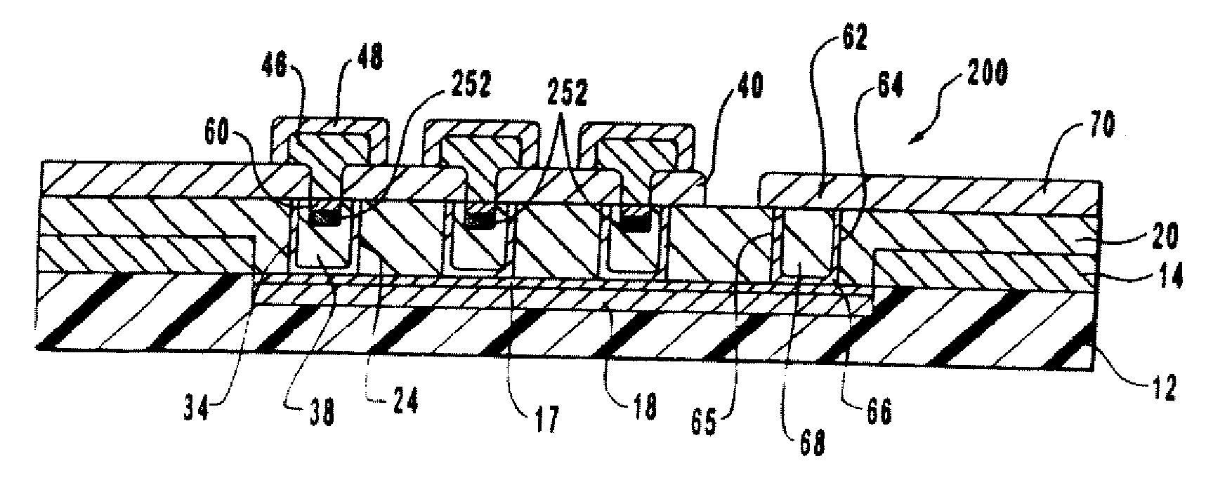
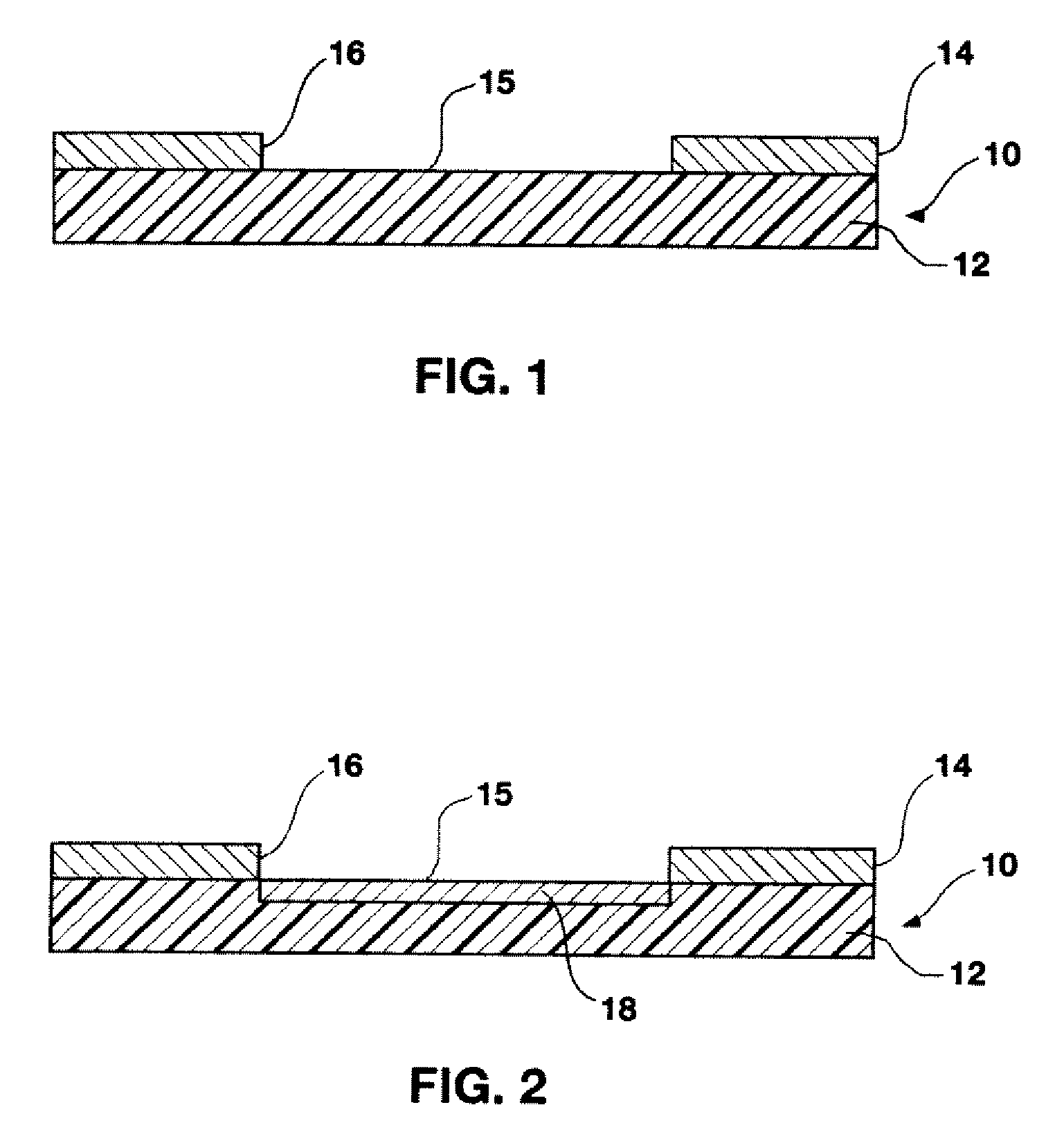
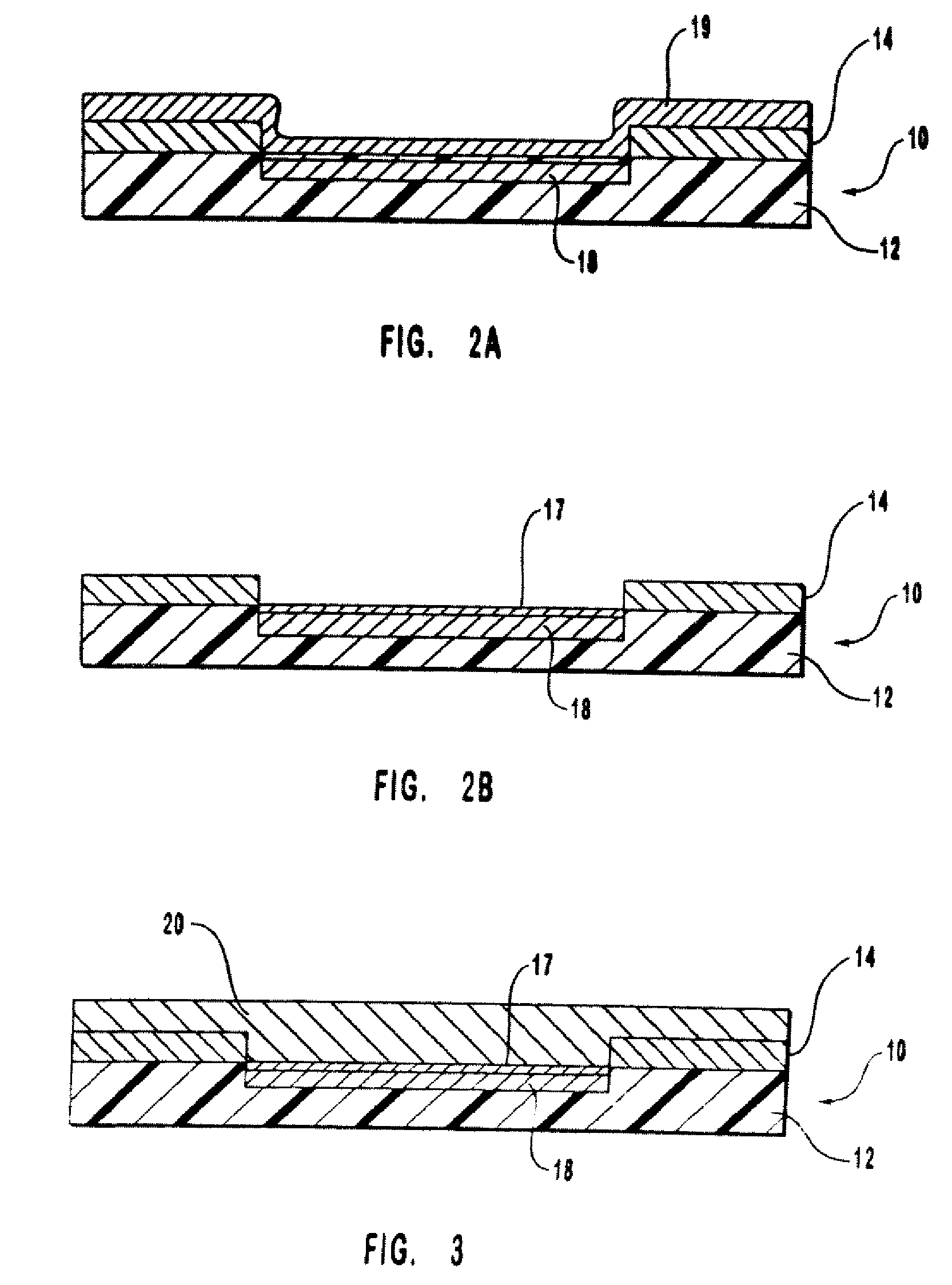
[0067] The present invention relates to improved vertical diodes and methods for manufacturing such diodes on a silicon wafer. Depicted in FIG. 1 is a layered wafer 10 used in constructing one embodiment of a vertical diode incorporating features of the present invention. Layered wafer 10 comprises a conventional silicon wafer 12 overlaid by an oxide layer 14. Silicon wafer 12 is doped with a first type dopant. As used in the specification and appended claims, the terms “first type dopant” and “second type dopant” can each refer either to an N-type dopant or a P-type dopant. However, once a convention is selected for manufacturing of a diode, the convention must be maintained. That is, either all first type dopants must be N doped and all second type dopants P doped, or all first type dopants must be P doped and all second type dopants N doped.

[0068] Oxide layer 14 is shown as having a hole 16 formed therethrough to expose a contact surface 15 on silicon wafer 12. Hole 16 can be fo...


PUM


Abstract

Semiconductor structures and methods of making a vertical diode structure are provided. The vertical diode structure may have associated therewith a diode opening extending through an insulation layer and contacting an active region on a silicon wafer. A titanium silicide layer may be formed over the interior surface of the diode opening and contacting the active region. The diode opening may initially be filled with an amorphous silicon plug that is doped during deposition and subsequently recrystallized to form large grain polysilicon. The silicon plug has a top portion that may be heavily doped with a first type dopant and a bottom portion that may be lightly doped with a second type dopant. The top portion may be bounded by the bottom portion so as not to contact the titanium silicide layer. In one embodiment of the vertical diode structure, a programmable resistor contacts the top portion of the silicon plug and a metal line contacts the programmable resistor.

Description

CROSS-REFERENCE TO RELATED APPLICATIONS [0001] This application is a continuation of application Ser. No. 11 / 210,401, filed Aug. 24, 2005, pending, which is a divisional of application Ser. No. 10 / 804,477, filed Mar. 19, 2004, now U.S. Pat. No. 7,166,875, issued Jan. 23, 2007, which is a continuation of application Ser. No. 10 / 104,240, filed Mar. 22, 2002, now U.S. Pat. No. 6,784,046, issued Aug. 31, 2004, which is a divisional of application Ser. No. 09 / 505,953, filed on Feb. 16, 2000, now U.S. Pat. No. 6,750,091, issued Jun. 15, 2004, which is a divisional of application Ser. No. 09 / 150,317, filed on Sep. 9, 1998, now U.S. Pat. No. 6,194,746, issued Feb. 27, 2001, which is a divisional of application Ser. No. 08 / 932,791, filed on Sep. 5, 1997, now U.S. Pat. No. 5,854,102, issued Dec. 29, 1998, which is a continuation of application Ser. No. 08 / 609,505, filed on Mar. 1, 1996, now abandoned All of the foregoing referenced patent applications and patents are being incorporated by ref...

Claims


Application Information

Patent Timeline
IPC IPC(8): H01L21/20H01L29/00H01L21/329H01L27/08H01L29/861
CPCH01L21/2022H01L27/0814H01L27/101H01L27/1021H01L27/24H01L29/6609Y10S438/979H01L29/861H01L45/04H01L45/145Y10S257/903Y10S257/91H01L29/66136H01L21/02667H01L21/02532H10B63/00H10N70/20H10N70/883
Inventor GONZALEZ, FERNANDOLOWREY, TYLER A.DOAN, TRUNG TRITURI, RAYMOND A.WOLSTENHOLME, GRAHAM R.
Owner MICRON TECH INC
Why Eureka
Try Eureka