
Semiconductor device

Inactive Publication Date: 2008-02-14
HITACHI LTD
View PDF12 Cites 2 Cited by
  • Summary
  • Abstract
  • Description
  • Claims
  • Application Information

AI Technical Summary

Benefits of technology

[0007]It is preferable that (2) the semiconductor substrate be an SOI substrate in (1). (3) The aforementioned heater may be a structure where a buried silicon oxide film of the SOI substrate is separated by an isolation groove in (2). Isolation of the heater can be more effectively performed by using the buried silicon oxide film of the SOI substrate. Isolation of the heater is effective as a result of the sidewall and the buried silicon oxide film.
[0008]In any of (1) to (3), it is preferable that (4) the aforementioned heating element be a bipolar transistor. By using the heating element of the semiconductor itself as a heater, isolation becomes possible even when it is a simple structure.
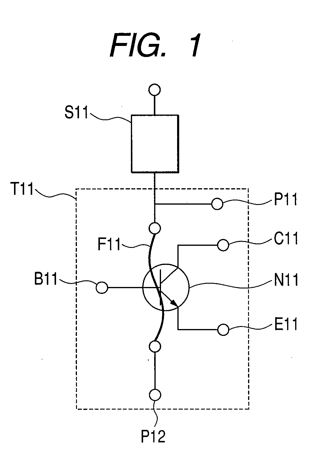
[0010]A semiconductor device according to the present invention includes a trimming element including a heating element formed over an SOI substrate, etc., an isolation groove which separates the heating element, and a fuse part consisting of a conductor film which is formed over the heating element through an insulation film. In a semiconductor device of the present invention, the heater is surrounded by isolation grooves formed of a silicon oxide film with a small thermal conductivity and a buried silicon oxide film of the SOI substrate, and, moreover, the exothermic efficiency is improved by arranging the heaters in parallel.
[0011]Trimming a highly accurate resistance, etc. becomes possible by using an isolated heater and fuse, and the fuse can be cut stably and easily by heating the heater and energizing the fuse part. As a result, highly reliable trimming becomes possible.

Problems solved by technology

However, this trimming method needs a step for forming a polycrystalline silicon film resistance element for a heater and variations in dimension may result because of, for instance, exposure conditions, etc. in the patterning process of the polycrystalline silicon film, so that there is a problem of the trimming yield becoming worse.

Method used


Image

  • Semiconductor device
  • Semiconductor device
  • Semiconductor device

Examples


first embodiment

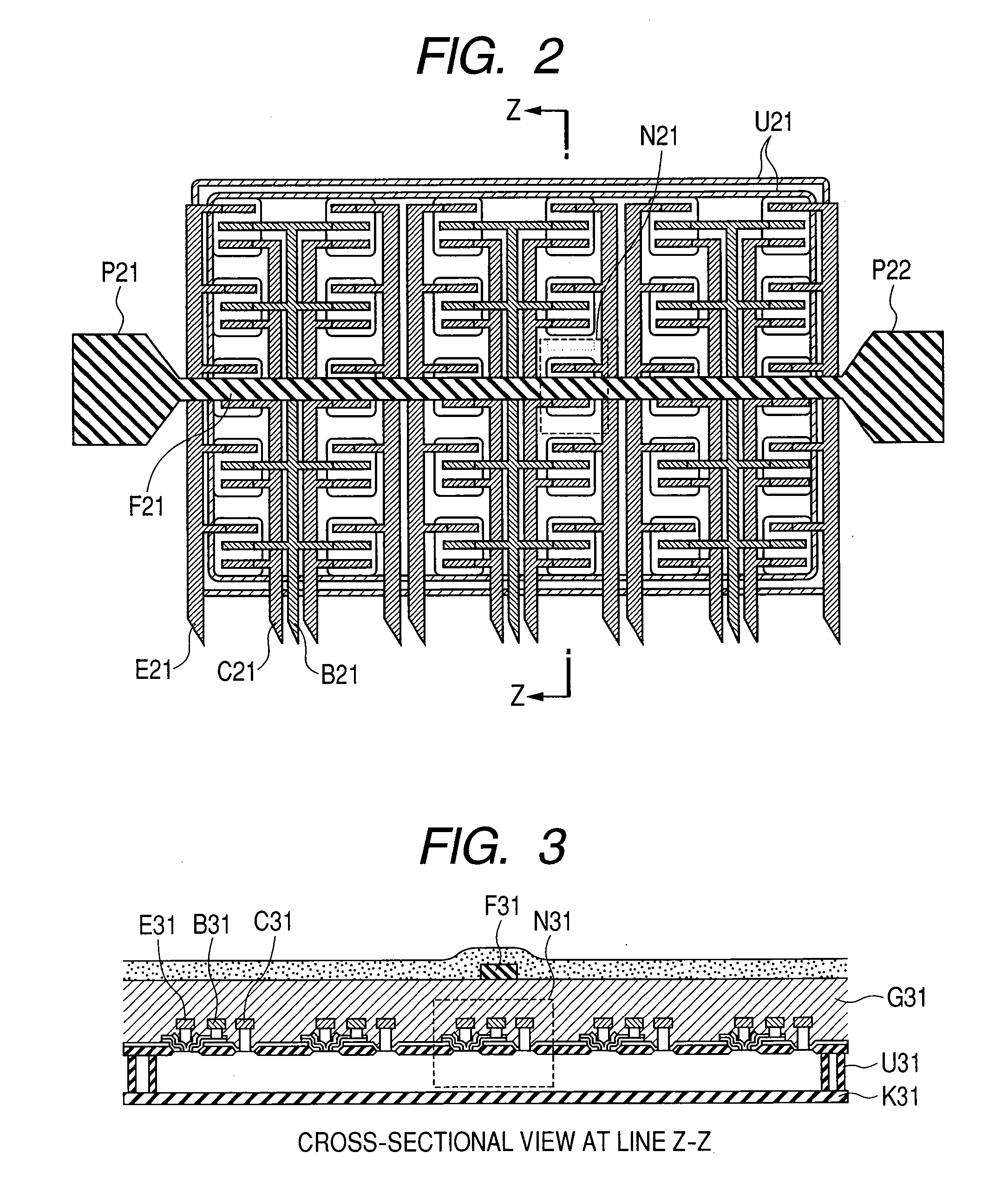
[0018]FIGS. 2 and 3 show one embodiment of a trimming element which is an example of a semiconductor device to which the present invention is applied. A plurality of bipolar transistors N21 / N31 are formed in parallel as heating elements over the SOI substrate, and, surrounding it, single or multiple isolation grooves U21 / U31 are formed of a silicon oxide film, etc. Moreover, a fuse part F21 / F31 is formed of a metallic film such as Al, etc. over the bipolar transistors N21 / N31 through an insulation film G31 composed of a silicon oxide film, etc. The bipolar transistors N21 / N31 for heating are separated from the buried silicon oxide film K31 of the SOI substrate by the isolation grooves U21 / U31. The bipolar transistors for heating formed in the isolation grooves are energized by applying a voltage to the electrodes B21 / B31, E21 / E31, and C21 / C31 to heat up the bipolar element intentionally, and, at the same time, a current flows between the input terminals P21 and P22 of both ends of t...

second embodiment

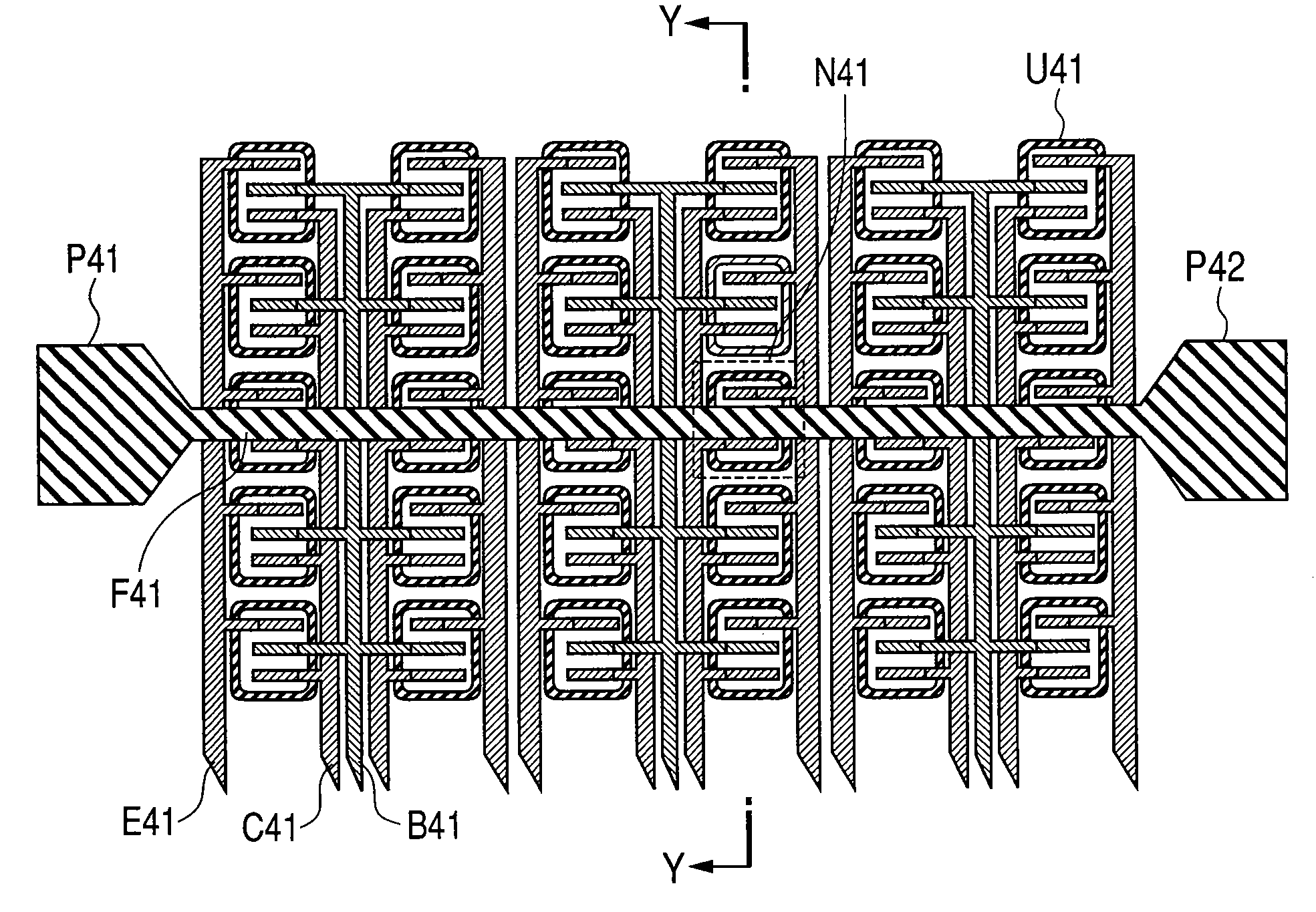
[0019]FIGS. 4 and 5 show another embodiment of a trimming element. A plurality of bipolar transistors N41 / N51 are formed in parallel as heating elements over the SOI substrate, and an individual transistor is separated by the isolation grooves U41 / U51. A fuse part F41 / F51 is formed of a metallic film such as Al, etc. over the bipolar transistors N41 / N51 through an insulation film G51 composed of a silicon oxide film, etc. the same as the first embodiment. Each bipolar transistor N41 / N51 is separated from the buried silicon oxide film K51 of the SOI substrate by the individual isolation grooves U41 / U51.


PUM


Abstract

A trimming element for trimming a redundant circuit and a high-accuracy resistance in consideration of the stability and the ease of fuse cutting, and more specifically a trimming element which is easily formed by an existing process. An SOI substrate, a heater connected to the SOI substrate, and a fuse connected to the heater are formed.

Description

CLAIM OF PRIORITY[0001]The present application claims priority from Japanese application JP 2006-217715 field on Aug. 10, 2006, the content of which is hereby incorporated by reference into this application.FIELD OF THE INVENTION[0002]The present invention relates to a semiconductor device and, specifically, relates to a structure of a trimming element supplied to trim a redundant circuit and a high-accuracy resistance, etc.BACKGROUND OF THE INVENTION[0003]A fuse cutting method is well known as a trimming technique for a redundant circuit and a high-accuracy resistance, etc. A method is used as a fuse cutting method, in which a fuse part formed of a metallic lead line and polycrystalline silicon, etc. is fused by irradiating a laser beam thereto and cut by applying a current. The current application method is adopted as an efficient trimming technique because fuse cutting can be done by common use of an element measuring device. JP-A No. 2003-78013 is a document describing a trimmin...

Claims


Application Information

Patent Timeline
IPC IPC(8): H01L29/00
CPCH01L23/5256H01L27/1203H01L27/0802H01L2924/0002H01L2924/00
Inventor NONAMI, HIDEAKI
Owner HITACHI LTD
Learn More