Semiconductor memory device

Active Publication Date: 2008-02-14
MICRON TECH INC
View PDF6 Cites 19 Cited by
  • Summary
  • Abstract
  • Description
  • Claims
  • Application Information

AI Technical Summary

Benefits of technology

[0026]As described above, according to the present invention, a row of sense amplifiers attached to a unit block can be used as a cache memory in a semiconductor memory device, and saving operation and write back operation are performed by switching control. Therefore, stored data can be prevented from being destroyed even when performing refresh operation. Thus, a large number of rows sense amplifiers can be effectively used as cache memories without being

Problems solved by technology

In this case, when the row of sense amplifiers attached to the unit block is being used as a sense amplifiers cache, the stored data in the sense amplifiers cache at that time is destroyed in the refresh operation.
As a consequence, it is a problem that the sense amplifiers cache cannot be used

Method used


Image

  • Semiconductor memory device
  • Semiconductor memory device
  • Semiconductor memory device

Examples


first embodiment

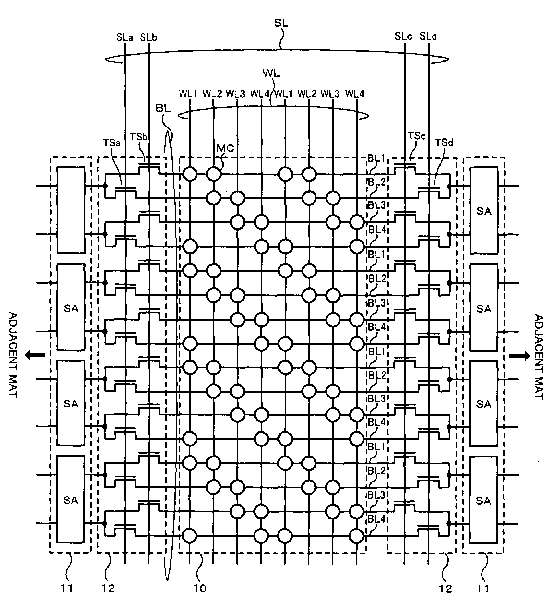
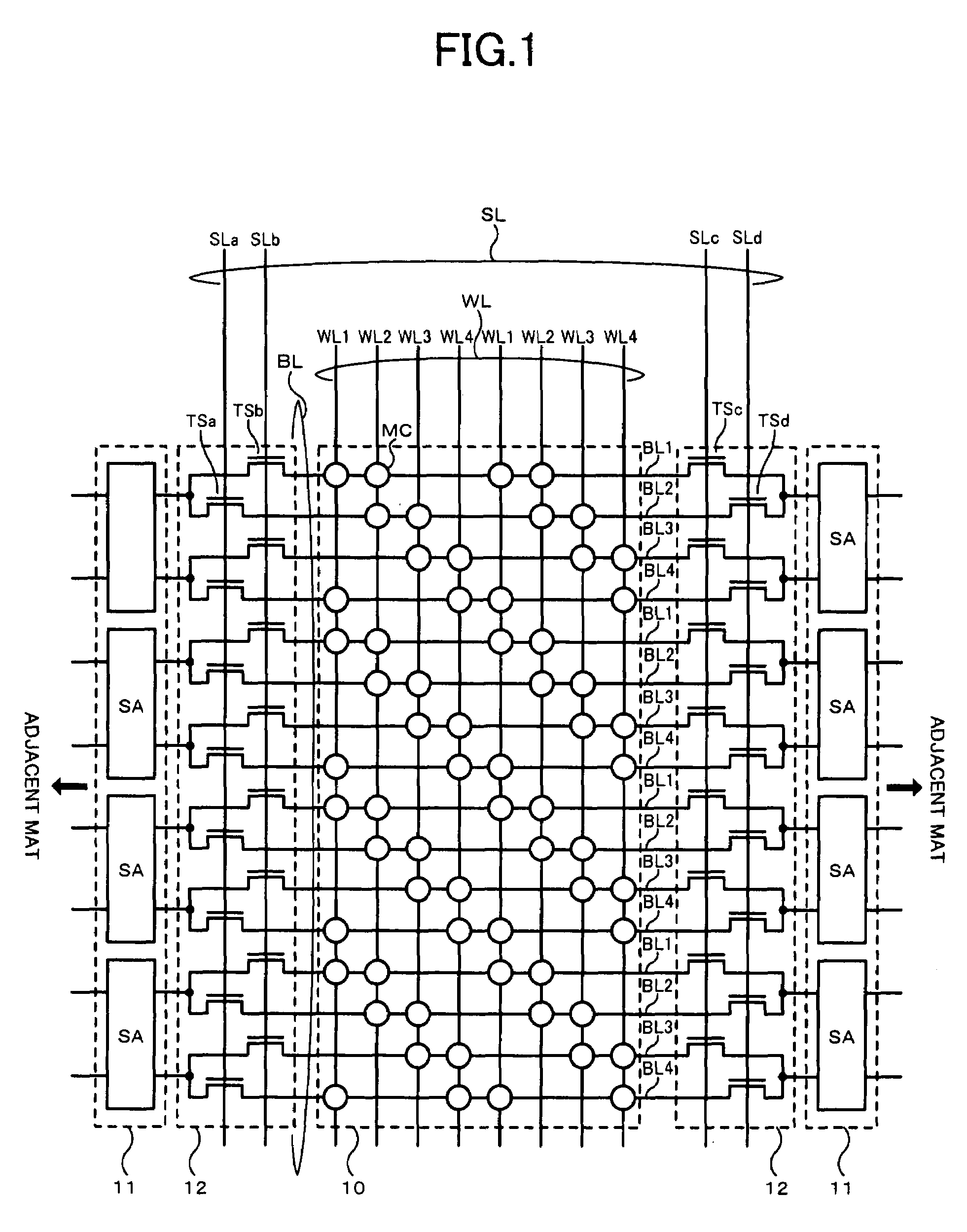
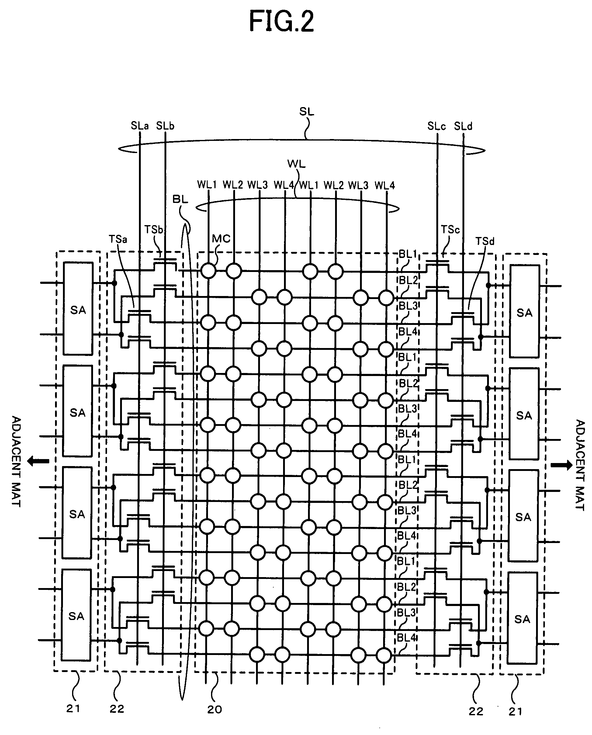
[0065]A first embodiment of the present invention will be described. FIGS. 1 and 2 show two types of configurations including a memory mat 10 as a unit block which is obtained by dividing a memory cell array of the DRAM of the first embodiment and its peripheral portion. In the first embodiment, a shared sense amplifier scheme is assumed in which adjacent memory mats 10 share sense amplifiers. FIG. 1 shows a configuration called ¼ pitch cell array configuration, and FIG. 2 shows a configuration called ½ pitch cell array configuration, respectively to which the shared sense amplifier scheme is applied.

[0066]First, the ¼ pitch cell array configuration will be described. In FIG. 1, a memory mat 10 is formed within a range including a plurality of word lines WL and a plurality of bit lines BL intersecting therewith. Although FIGS. 1 and 2 show an example in which a single memory mat 10 includes eight word lines WL and sixteen bit lines BL, generally a memory mat 10 of a desired size inc...

second embodiment

[0129]A second embodiment of the present invention will be described. The configuration shown in FIGS. 1 to 7 of the first embodiment is common to a DRAM of the second embodiment, so description thereof will be omitted. Meanwhile, a block diagram of FIG. 29 shows a schematic configuration of the DRAM of the second embodiment. By comparing the configuration of FIG. 29 with that of FIG. 8, a difference exists in that special purpose cache memories 70a and 70b attached to the memory cell array are provided. That is, the cache memory 70a between the row of sense amplifier 11a and one column decoder 61a is provided at the left side of FIG. 29, while the cache memory 70b between the row of sense amplifier 11e and the other column decoder 61b is provided at the right side of FIG. 29. Thus, the five rows of sense amplifiers ha to 11e are not used as the cache memories in the second embodiment. Moreover, other elements in the configuration are common to those in FIG. 8.

[0130]FIG. 30 is a con...

third embodiment

[0143]A third embodiment of the present invention will be described. In the third embodiment, the configuration and control on the basis of the first or the second embodiment can be applied, in which the row of sense amplifiers 11 is not used as the sense amplifier cache and is used for the purpose of data transfer between the rows of sense amplifiers 11 of different memory mats 10. In the following, a case in which control of the third embodiment is applied to the DRAM of the first embodiment will be described.

[0144]FIG. 35 is a connection state diagram when performing data transfer from the memory mat 10b at the second from the left to the memory mat 10d at the right end. In FIG. 35, data of the memory cells MC on a predetermined word line WL of the memory mat 10b is assumed to be stored in the rows of sense amplifiers 11b and 11c attached to the memory mat 10b. First, switch control for forming a first transfer path from the row of sense amplifiers 11c at the right side of the me...


PUM


Abstract

A semiconductor memory device of the invention comprises unit blocks into which the memory cell array is divided, rows of sense amplifiers arranged at one end and the other end of the plurality of bit lines in the unit block, switch means for switching a connection state between the unit block and the row of sense amplifiers attached to the unit block; and control means for controlling the switch means so as to form a transfer path from the row of sense amplifiers attached to a predetermined the unit block leading to the row of sense amplifiers as a saving destination not attached to the predetermined the unit block. This row of sense amplifiers attached to the predetermined the unit block functions as a cache memory.

Description

BACKGROUND OF THE INVENTION[0001]1. Field of the Invention[0002]The present invention relates to a semiconductor memory device which rewritably stores data in a memory cell array divided into unit blocks, and particularly relates to a semiconductor memory device having a configuration of storing data of the unit blocks in a cache memory.[0003]2. Description of the Related Art[0004]Generally, a semiconductor memory device such as a DRAM has a configuration in which a memory cell array is divided into a plurality of banks and each bank is further divided into a plurality of unit blocks. Data is stored in a plurality of memory cells formed at intersections between a plurality of word lines and a plurality of bit lines in each unit block. For example, a row of sense amplifiers including a plurality of sense amplifiers is generally arranged on each of both sides of the unit block. Further, a configuration in which switches are provided between each unit block and each row of sense amplif...

Claims


Application Information

Patent Timeline
IPC IPC(8): G11C8/12
CPCG11C8/10G11C11/4091G11C11/4093G11C2207/005G11C2207/2245G11C8/08G06F2212/1016G06F2212/3042G11C7/065G11C7/1039G11C7/18G06F12/0893
Inventor KAJIGAYA, KAZUHIKO
Owner MICRON TECH INC
Why Eureka
Try Eureka