Semiconductor bonding and layer transfer method

a layer transfer and semiconductor technology, applied in the field of semiconductors, can solve the problems of large chip area consumption of laterally oriented devices, large amount of chip area of processor circuits, and large amount of idle processor circuits for many cycle times,

Inactive Publication Date: 2008-02-14
BESANG
View PDF21 Cites 274 Cited by
  • Summary
  • Abstract
  • Description
  • Claims
  • Application Information

AI Technical Summary

Problems solved by technology

However, these laterally oriented devices consume significant amounts of chip area.
As a result, the processor circuit is idle for many cycle times while it accesses the main memory.
Hence, cache memory uses a small amount of fast and expensive memory to allow the processor circuit faster access to information normally stored by a large amount of slower, less-expensive memory.
There are several problems, however, with using 3-D packages and 3-D ICs.
One problem is that the use of wire bonds increases the access time between the processor and memory circuits because the impedance of wire bonds and large contact pads is high.
Similarly, the contact pads in 3-D ICs have correspondingly large capacitances which also increase the access time between the processor and memory circuits.
Another problem is that the use of wire bonds is less reliable because the wire bonds can break and become detached.
Another problem with using 3-D packages and 3-D ICs is cost.
The use of wire bonds is expensive because it is difficult to attach them between the processor and memory circuits and requires expensive equipment.
Further, it requires expensive equipment to align the various devices in the 3-D IC.
The bonding and alignment is made even more difficult and expensive because of the trend to scale devices to smaller dimensions.
As mentioned above, the SRAM cells are larger and expensive, so increasing the number of them in the memory circuit would increase the cost of the computer chip dramatically.
DRAM cells are less expensive and smaller, but to include them in the memory circuit will still increase the cost.
One reason the costs increase for both embedded SRAM and DRAM cells is because they both use a number of masks to fabricate them.
One problem with using lateral memory devices in the memory circuit is their size.
Hence, to increase the number of memory cells in the memory circuit, the DRAM or SRAM cells would have to be scaled to smaller dimensions, but this requires advances in lithography and increasingly expensive manufacturing equipment.
Further, the DRAM and SRAM cells become less accurate and reliable when scaled to smaller dimension.

Method used


Image

  • Semiconductor bonding and layer transfer method
  • Semiconductor bonding and layer transfer method
  • Semiconductor bonding and layer transfer method

Examples


Embodiment Construction

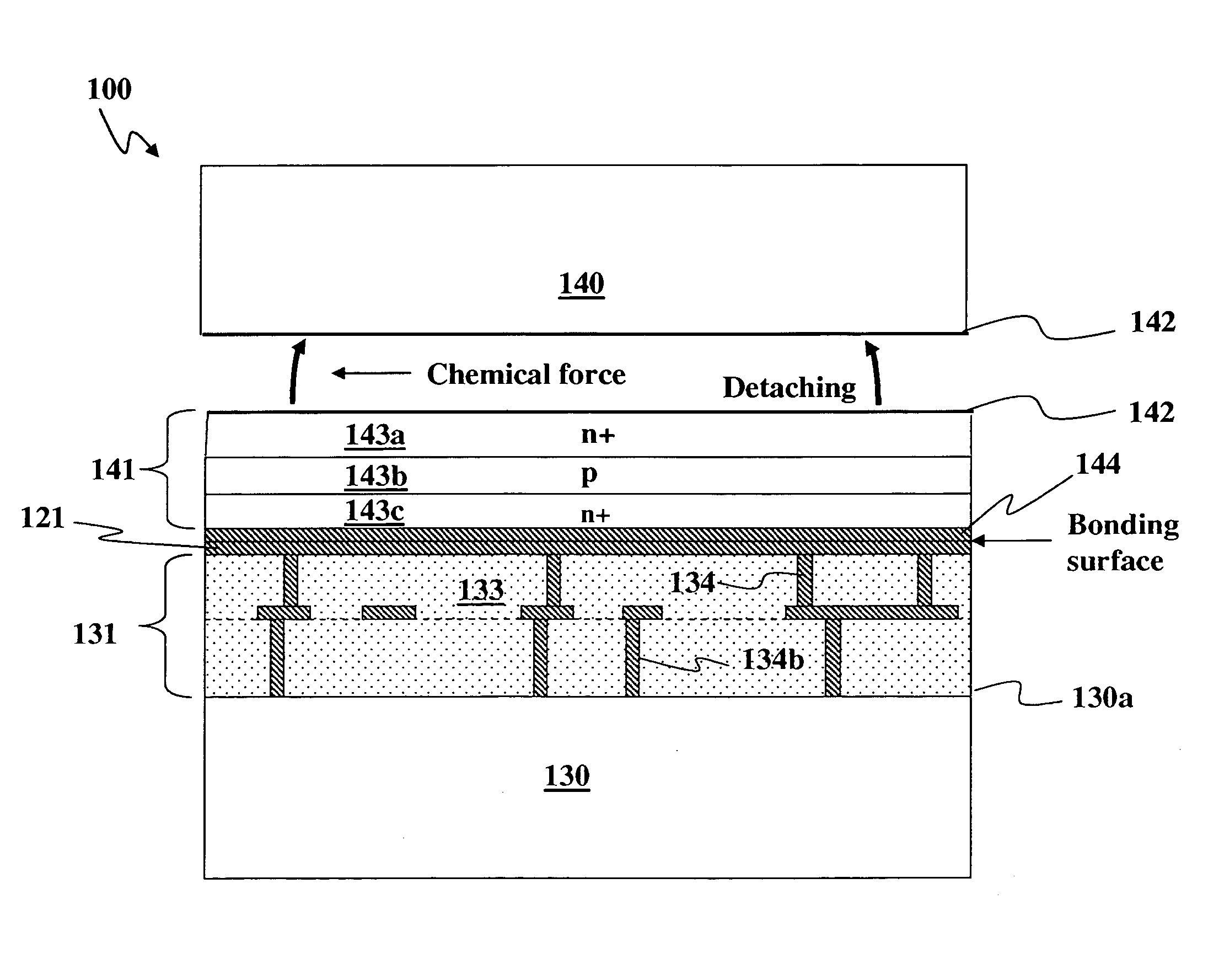
[0023]FIGS. 1-23 are simplified sectional views of steps in fabricating circuitry 100 using a semiconductor bonding transfer method in accordance with the present invention. It should be noted that in the following figures, like reference characters indicate corresponding elements throughout the several views. In this embodiment, circuitry 100 includes separate portions in which it is desired to bond them together. As will be discussed in more detail below, one portion is carried by an acceptor substrate and another portion is carried by a donor substrate. In accordance with the invention, the portion carried by the donor substrate is bonded to the portion carried by the acceptor substrate and then the donor substrate is removed. It should be noted that the portions carried by the donor and acceptor substrates can have many different configurations, but only a few are discussed herein.

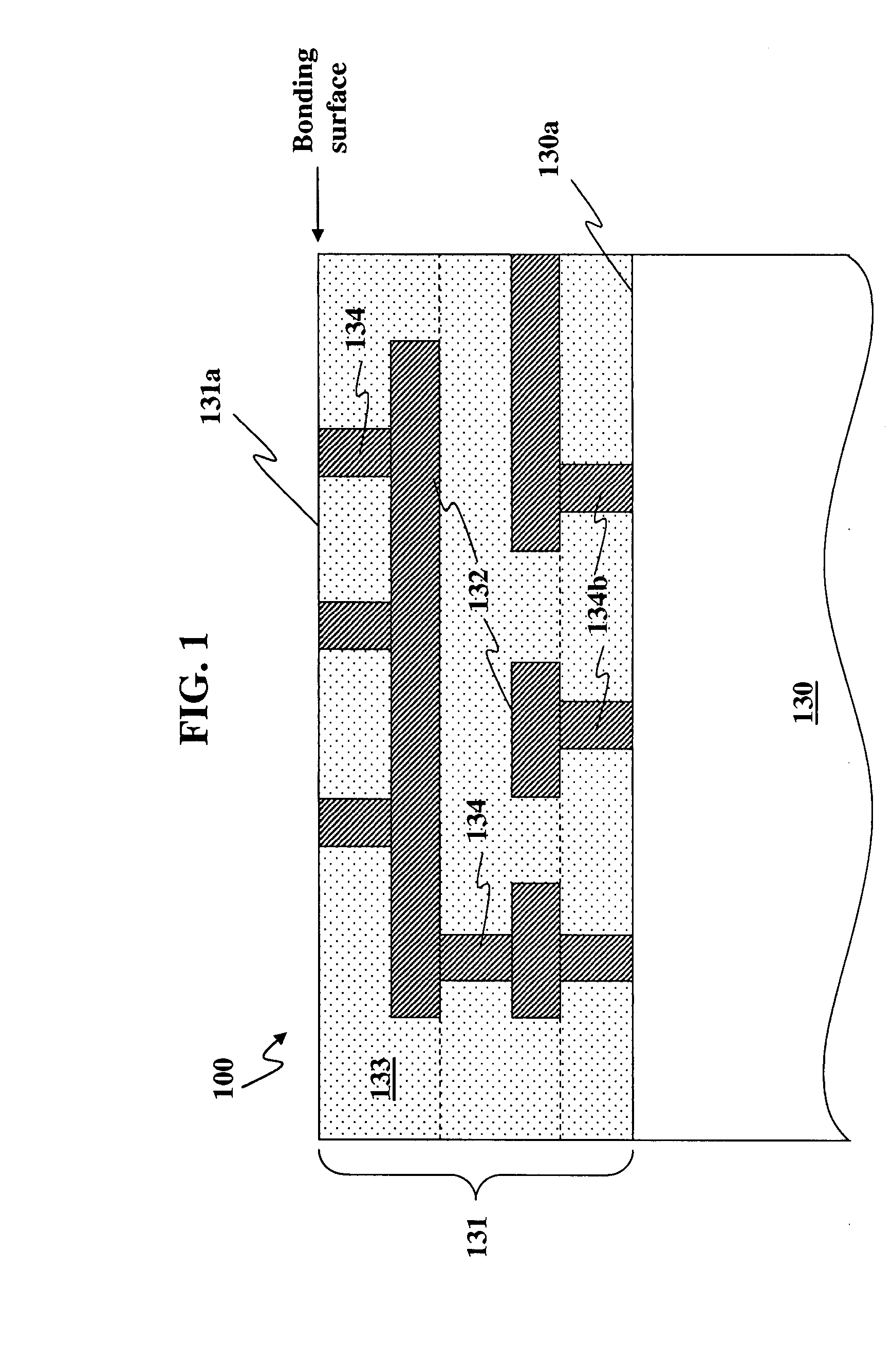
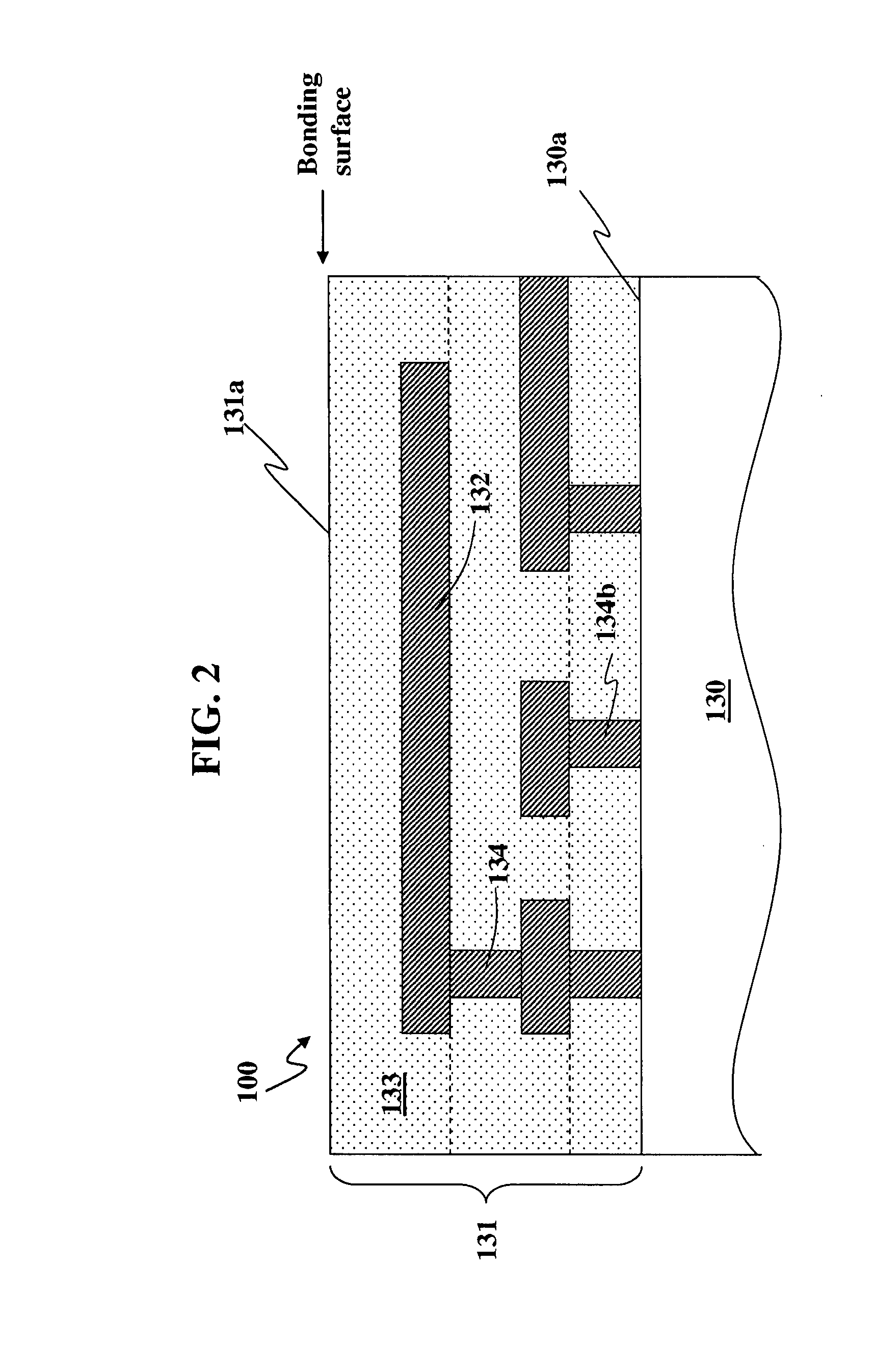
[0024] The portions carried by the acceptor substrate are shown in FIGS. 1-5 and the portions carr...


PUM


Abstract

The present invention provides a method of coupling substrates together. The method includes providing first and second substrates and then coupling the first and second substrates together. One of the first and second substrates includes devices with an interconnect region positioned thereon and the other substrate carries a device structure.

Description

CROSS REFERENCE TO RELATED APPLICATIONS [0001] This is a divisional of application Ser. No. 11 / 092,501, entitled “SEMICONDUCTOR BONDING AND LAYER TRANSFER METHOD”, filed on Mar. 29, 2005, which claims priority to U.S. Pat. No. 7,052,941 filed on Jun. 21, 2004, the contents of both of which are incorporated herein by reference.BACKGROUND OF THE INVENTION [0002] 1. Field of the Invention [0003] The present invention relates generally to semiconductors and, more particularly, to forming circuitry using wafer bonding. [0004] 2. Description of the Related Art [0005] Advances in semiconductor manufacturing technology have provided computer chips with integrated circuits that include many millions of active and passive electronic devices, along with the interconnects to provide the desired circuit connections. As is well-known, most integrated circuits include laterally oriented active and passive electronic devices that are carried on a single major surface of a substrate. Active devices ...

Claims


Application Information

Patent Timeline
Patent Type & Authority Applications(United States)
IPC IPC(8): H01L21/30H01L21/20H01L21/336H01L21/46H01L21/58H01L23/48H01L27/108H01L27/148
CPCH01L21/187H01L21/2007H01L2924/1305H01L2924/1301H01L27/1052H01L2924/0132H01L2924/01033H01L24/29H01L2924/3011H01L2924/30105H01L2924/19043H01L21/6835H01L21/76829H01L24/83H01L27/0688H01L27/1027H01L27/105H01L27/11H01L27/1116H01L27/11551H01L2221/68368H01L2224/291H01L2224/8385H01L2924/01005H01L2924/01013H01L2924/01015H01L2924/01018H01L2924/01027H01L2924/01029H01L2924/01038H01L2924/01049H01L2924/01056H01L2924/01073H01L2924/01074H01L2924/01075H01L2924/01078H01L2924/01079H01L2924/01093H01L2924/07802H01L2924/09701H01L2924/13091H01L2924/14H01L2924/1433H01L2924/19041H01L2924/19042H01L2924/01006H01L2924/01014H01L2924/01031H01L2924/00H01L23/48H10B99/00H10B10/18H10B10/00H10B41/20
Inventor LEE, SANG-YUN
Owner BESANG
Why Eureka
Try Eureka