Supercharge Your Innovation With Domain-Expert AI Agents!

Integrated circuit

a technology of integrated circuits and integrated circuits, applied in the field of integrated circuits, can solve the problems of increasing the size of the integrated circuit chip, increasing the storage capacity, and wasting time in inputting unnecessary data and outputting, so as to reduce the chip size and test time

Inactive Publication Date: 2008-02-21
SOCIONEXT INC
View PDF12 Cites 4 Cited by
  • Summary
  • Abstract
  • Description
  • Claims
  • Application Information

AI Technical Summary

Benefits of technology

[0013]The present invention was made under the background circumstances described above. An object of the present invention is to provide an integrated circuit that enables a reduction in chip size and test time.

Problems solved by technology

With such a test system, however, the following problems arise.
As a result, storage capacity wasted increases and time is wasted in inputting unnecessary data and outputting and determining meaningless data.
Therefore, the size of an integrated circuit chip increases and test time lengthens.

Method used


Image

  • Integrated circuit
  • Integrated circuit
  • Integrated circuit

Examples


first embodiment

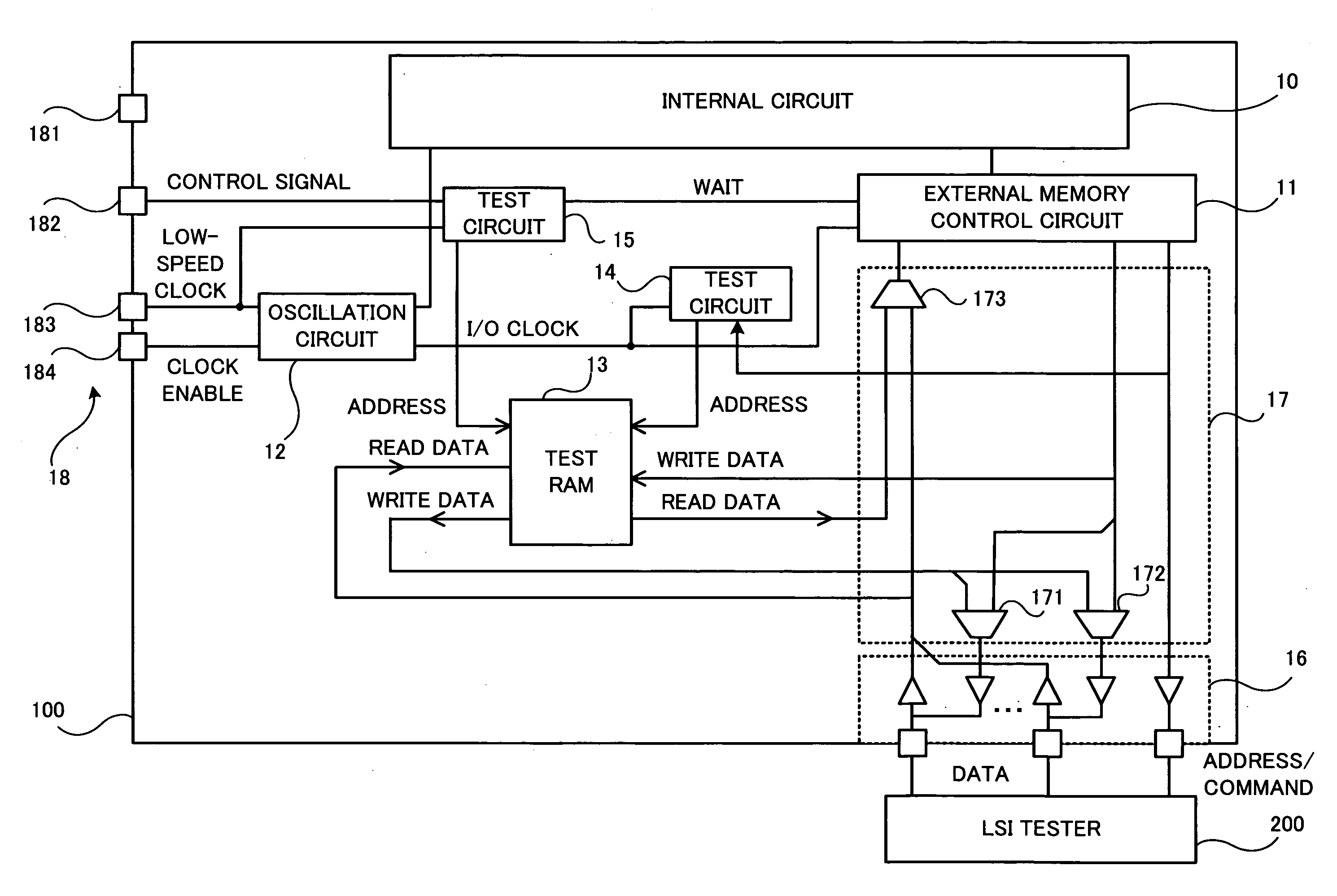
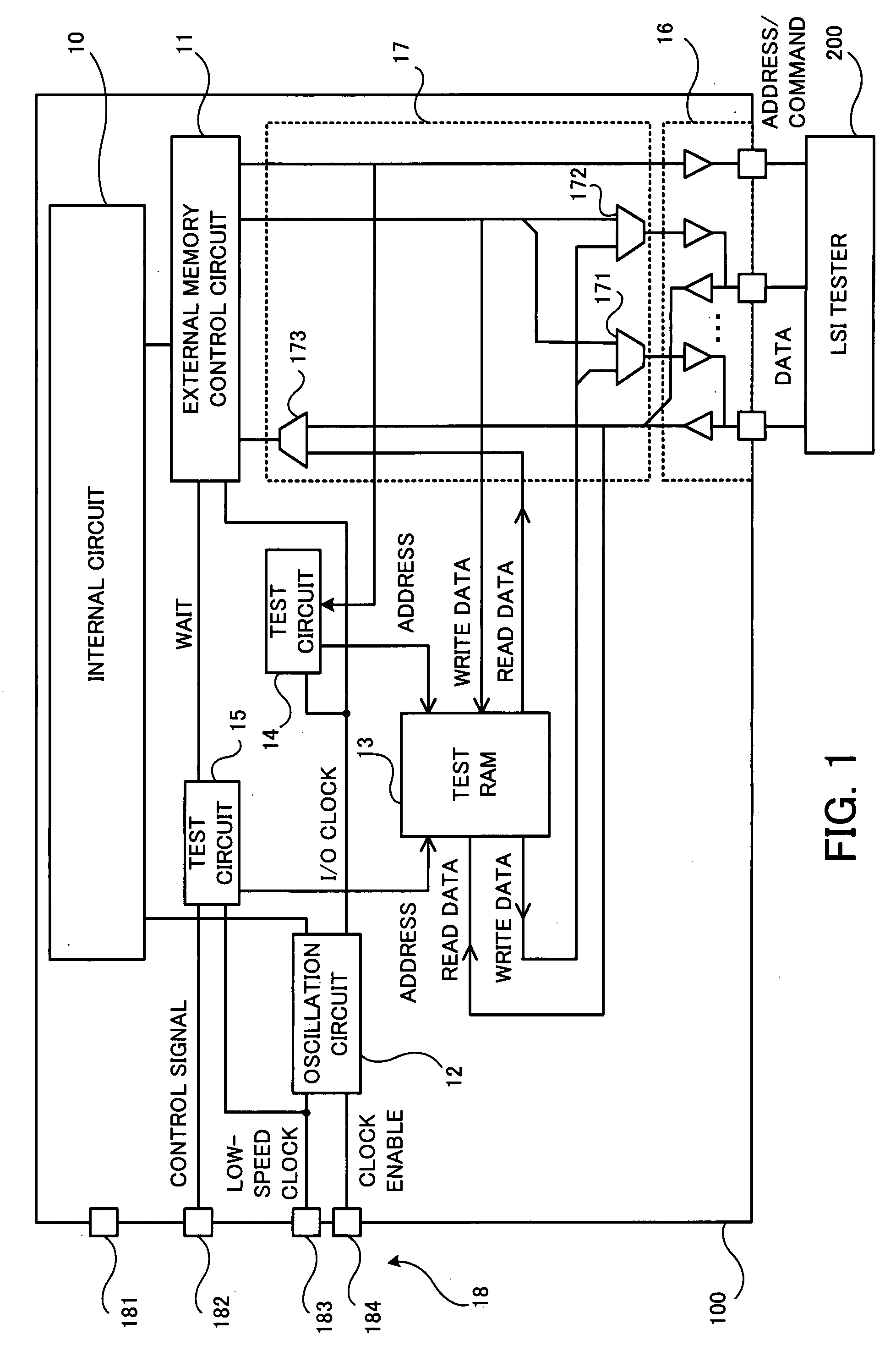
[0045]FIG. 1 is a block diagram showing a system according to the present invention.

[0046]A system according to a first embodiment of the present invention comprises an integrated circuit 100 and an LSI tester 200.

[0047]The LSI tester 200 is used for testing the operation of the integrated circuit 100 and inputs various test signals to a plurality of terminals of the integrated circuit 100.

[0048]The integrated circuit 100 includes an internal circuit 10, an external memory control circuit 11, an oscillation circuit 12, a test RAM 13, test circuits 14 and 15, an I / O 16, a test selector 17, and a test signal input section 18.

[0049]The internal circuit 10 is a circuit to be measured.

[0050]The external memory control circuit 11 outputs a command to the test circuit 14 and exchanges data with the test RAM 13.

[0051]Furthermore, the external memory control circuit 11 exchanges data (read data and write data) and the like with the LSI tester 200 via the I / O 16 by using an address / command (r...

second embodiment

[0076]A system according to the present invention will now be described.

[0077]The differences between the systems according to the first and second embodiments of the present invention will mainly be described and descriptions of the same matters will be omitted.

[0078]FIG. 4 is a block diagram showing the system according to the second embodiment of the present invention.

[0079]An integrated circuit 100a according to the second embodiment of the present invention differs from the integrated circuit 100 according to the first embodiment of the present invention in that low-speed data input-output terminals and high-speed data input-output terminals are separated. The integrated circuit 100a includes a test selector 17a in place of the test selector 17 and includes an I / O 19 and an input section 20.

[0080]The test selector 17a does not include selectors 171 and 172 but includes a plurality of selectors (selectors 174 and 175, in this example) for performing switching between the outputt...

third embodiment

[0086]A system according to the present invention will now be described.

[0087]The differences between the systems according to the second and third embodiments of the present invention will mainly be described and descriptions of the same matters will be omitted.

[0088]FIG. 5 is block diagram showing the system according to the third embodiment of the present invention.

[0089]An integrated circuit 100b according to the third embodiment of the present invention differs from the integrated circuit 100a according to the second embodiment of the present invention in that it includes an I / O 19a in which terminals for inputting read data and terminals for outputting write data are separated.

[0090]The same effect that is obtained by the system according to the second embodiment of the present invention can be achieved by the system according to the third embodiment of the present invention. In addition, with the system according to the third embodiment of the present invention the input term...


PUM


Abstract

An integrated circuit that enables a reduction in chip size and test time. This integrated circuit comprises an internal circuit; an external memory control circuit for inputting read data from an LSI tester by the use of a read command and for outputting write data to the LSI tester by the use of a write command; a test RAM including a read data storage section for storing the read data inputted from the LSI tester at a low speed and a write data storage section for storing the write data outputted from the control circuit; a test circuit for interpreting the read command and the write command issued by the external memory control circuit, for supplying, at the time of determining that the read data must be inputted to the external memory control circuit, the read data from the test RAM to the external memory control circuit at a high speed, and for supplying, at the time of determining that the write data is outputted from the external memory control circuit, the write data outputted from the external memory control circuit to the test RAM at a high speed; and a test circuit for outputting the write data stored in the test RAM to the LSI tester at a low speed.

Description

CROSS-REFERENCE TO RELATED APPLICATIONS[0001]This application is based upon and claims the benefits of priority from the prior Japanese Patent Application No. 2006-223281, filed on Aug. 18, 2006, the entire contents of which are incorporated herein by reference.BACKGROUND OF THE INVENTION[0002](1) Field of the Invention[0003]This invention relates to an integrated circuit and, more particularly, to an integrated circuit capable of verifying the operation speed of a circuit.[0004](2) Description of the Related Art[0005]In recent years there have been many cases where an ordinary semiconductor integrated circuit to which a high-speed random access memory (RAM) is externally connected is used. The high-speed RAM is a RAM in which a data input-output rate is higher than the rate of an ordinary semiconductor tester, or a RAM the operation speed of which is so high that data which is outputted from the semiconductor integrated circuit and which is synchronized with a clock cannot be input...

Claims


Application Information

Patent Timeline
IPC IPC(8): G11C7/00
CPCG11C29/14
Inventor ISHIKAWA, KATSUYAOTSUKA, TATSUSHI
Owner SOCIONEXT INC
Features
  • R&D
  • Intellectual Property
  • Life Sciences
  • Materials
  • Tech Scout
  • Unparalleled Data Quality
  • Higher Quality Content
  • 60% Fewer Hallucinations
Learn More