Driver apparatus and method

a technology of driving apparatus and driver, which is applied in the direction of electric variable regulation, process and machine control, instruments, etc., can solve the problems of minimal power consumption, impractical large devices for mnb>1/b> and cdac devices, and easy damage, etc., and achieve the effect of maximum curren

Active Publication Date: 2008-02-28
CIRRUS LOGIC INC
View PDF12 Cites 44 Cited by
  • Summary
  • Abstract
  • Description
  • Claims
  • Application Information

AI Technical Summary

Benefits of technology

[0028] According to a further aspect of the invention, a current detector is provided for monitoring the flow of current in the shunt path, the current detector being configured to limit the flow of current through a light source. This further aspect of the invention

Problems solved by technology

Due to the requirement of having the maximum possible voltage drop across the LEDs, and the minimum voltage drop across the current source IS1, the circuit of FIG. 11a is susceptible to damage due to the high voltage at Node A of FIG. 5.
Such an offset will, because of the high gain (gm) of MN2, result in errors.
But since the off

Method used


Image

  • Driver apparatus and method
  • Driver apparatus and method
  • Driver apparatus and method

Examples


first embodiment

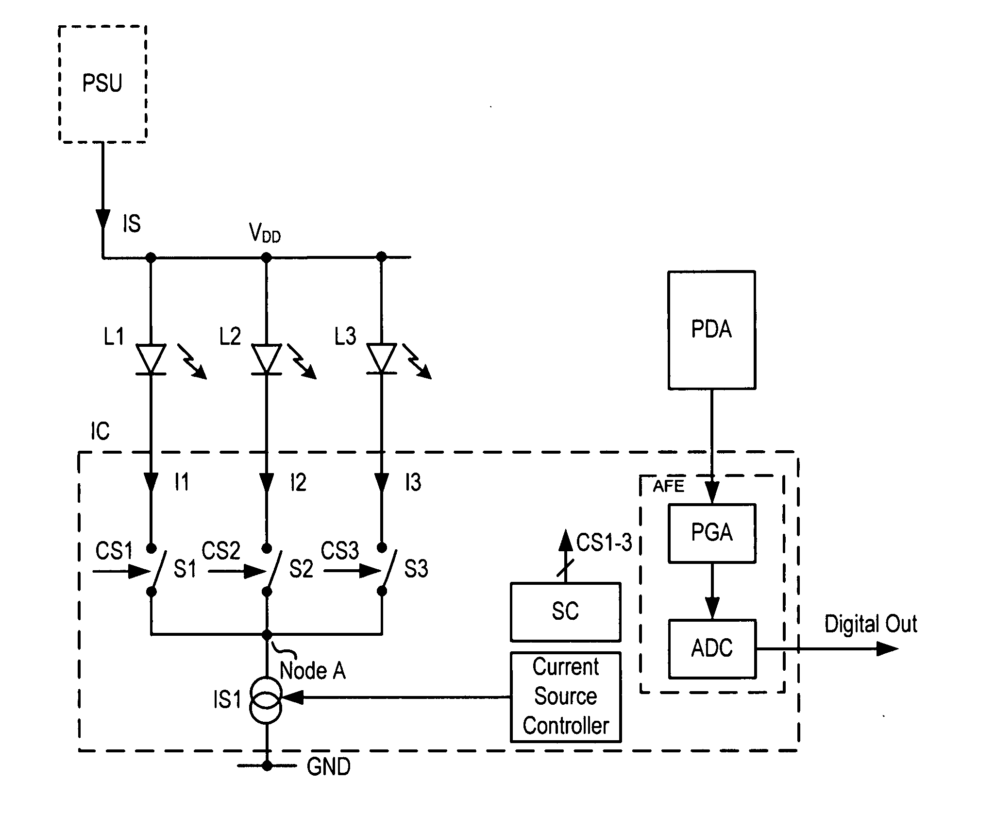
[0052] Thus, it can be seen that in the first embodiment the LED switches (S1-S3) may be integrated on the same IC as the AFE processing circuitry, with the current source IS1 being provided to reduce the generation of unwanted transient signals.

second embodiment

[0053]FIG. 5 shows a basic block diagram of the present invention.

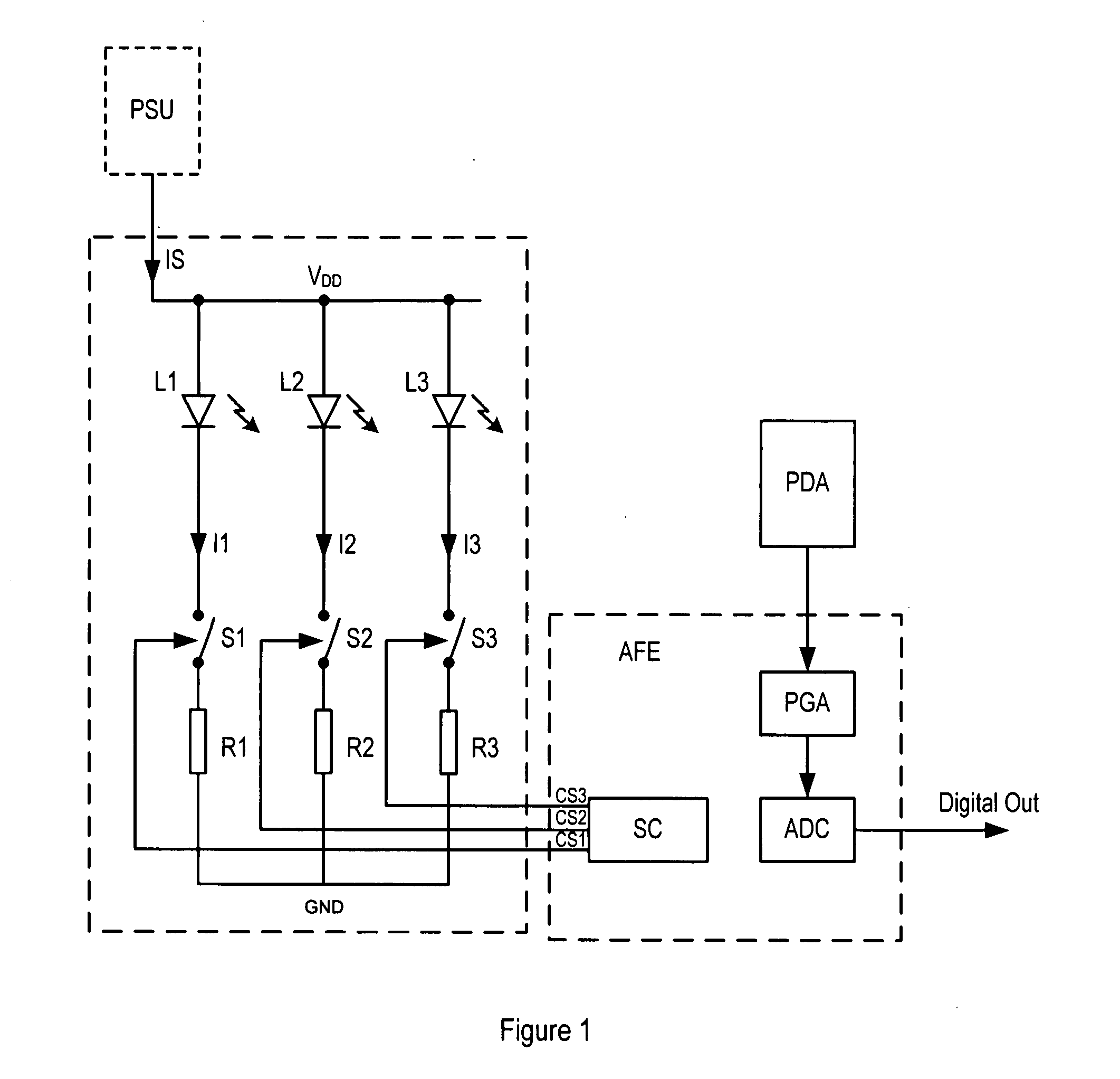
[0054] In a similar manner to FIG. 3, an LED array comprises Red, Green and Blue LEDs L1, L2, L3. The LED switching circuitry S1, S2, S3 is placed on the same monolithic circuit as the analogue front end circuitry (AFE) that drives the switching circuitry. A current source IS1 is provided in the current path between the switches S1, S2, S3 and ground, for controlling the flow of current through the LEDs L1, L2, L3.

[0055] According to the second embodiment a shunt path 50 is provided. The shunt path 50 comprises a switching device S4. The shunt path 50 having the switching device S4 is provided in parallel with the LED array and switching circuitry. The problem relating to the LED switching transients interfering with the ADC is reduced because, as will be explained below, the shunt path 50 enables harmful transitions in the ground current flow to be reduced.

[0056] The following text describes the operation of the sw...

third embodiment

[0076]FIG. 8 shows a basic diagram of a third embodiment according to the present invention.

[0077] As with FIGS. 3 and 5, an LED array comprises Red, Green and Blue LEDs L1, L2, L3. The LED switching circuitry S1, S2, S3 may form part of the same monolithic circuit as the analogue front end circuitry (AFE) that processes the image data received from the photo sensors. To reduce the problem associated with LED switching transients interfering with the ADC process, a current source IS1 is provided in the current path between the switches S1, S2, S3 and ground, for controlling the flow of current through the LEDs L1, L2, L3. A differential current path 50 (or shunt path) having a switching device S4 is provided in parallel with the array of LEDs and corresponding switches S1-S3.

[0078] In addition, according to this embodiment, a second current source IS2 is provided in the shunt path 50. The second current source IS2 enables the switching of the shunt path 50 to be performed in a more...


PUM


Abstract

A driver apparatus is provided for controlling a light source array comprising at least first and second light sources, the light source array used for illuminating a scan region on a target object, wherein light reflected from said target object is captured by a detector. The driver apparatus comprises a single integrated circuit comprising processing means for processing image data received from the detector, a switching array comprising at least first and second switches for switching the respective first and second light sources, and a current source for controlling the flow of current through the light sources. In this way the LED switching circuitry that controls an LED array is placed on the same integrated circuit (i.e. monolithic circuit) as the analogue processing circuitry that processes the image data, with the current source controlling the flow of current through the LEDs in the LED array. The current source has the advantage of avoiding rapid changes or slope discontinuities in the current flowing through the LEDs, which would otherwise cause unwanted transient signals. A shunt path comprising a switching device may be provided in parallel with the LED array and switching array. The shunt path has the advantage of enabling the switching sequence from one LED to another to be controlled such that a substantially constant current is drained from the supply (subject to any differences in the inherent current drawn by the Red, Green and Blue LEDs, respectively).

Description

TECHNICAL FIELD [0001] The present invention relates to a driver apparatus and method for driving light sources, and in particular, but not exclusively, to a RGB (Red, Blue, Green) LED Driver circuit that controls the current through light sources used for illuminating a target object, light from the target object being detected by a sensor, for example a CIS / CCD imaging sensor, as used in imaging apparatus such as optical imagers, i.e. scanners, and the like, and that is integrated on the same monolithic structure as analogue signal processing circuitry, commonly referred to as Analogue Front End (AFE) circuitry. BACKGROUND [0002]FIG. 1 shows a basic diagram of a state of the art LED driver circuit that is used, for example, in an image reading apparatus in conjunction with a CIS or CCD image sensor device. An LED array L1-L3 is coupled to switches S1-S3 and resistors R1-R3. The LED array L1-L3, switching circuit S1-S3, and resistors R1-R3 are arranged separately from the analogue ...

Claims


Application Information

Patent Timeline
IPC IPC(8): H05B37/02H05B44/00
CPCH04N1/40056H04N1/484Y02B20/347H05B33/0857H05B33/089H05B33/0818H05B45/20Y02B20/30H05B45/395H05B45/52
Inventor STEELE, COLINHEARNE, CATHERINE A.SINGLETON, DAVID P.
Owner CIRRUS LOGIC INC
Why Eureka
Try Eureka