
Production Method of Multilayer Electronic Device

a production method and electronic device technology, applied in the direction of capacitors, electrical devices, fixed capacitors, etc., can solve the problems of high short-circuiting defect rate, non-adhesion defects, insufficient adhesion force, etc., and achieve excellent stacking properties and low short-circuiting defect rate

Inactive Publication Date: 2008-03-06
TDK CORPARATION
View PDF9 Cites 11 Cited by
  • Summary
  • Abstract
  • Description
  • Claims
  • Application Information

AI Technical Summary

Benefits of technology

The present invention relates to a production method of a low-cost multilayer electronic device, such as a multilayer ceramic capacitor, with excellent stacking property and reduced nonadhesion defects and short-circuiting defects, even when the green sheet is made very thin. The invention aims to provide a method that can produce a thinner green sheet with good adhesion and reduced nonadhesion and short-circuiting defects, while also responding to demands for further thinner layers.

Problems solved by technology

However, when directly stacking the green sheets each having an internal electrode pattern thereon as in the patent article 1, there has been a disadvantage that an adhesive force becomes insufficient between the internal electrode formation surface and a green sheet surface, and nonadhesion defects arise.
Furthermore, when the internal electrodes are made thinner, a short-circuiting defect rate becomes high.
However, in this method, the green sheet layer has to be made extremely thin as about half thickness of the desired thickness, so that it has been difficult to respond to demands for further thinner layers.
However, in the method disclosed in these articles, each green sheet layer has to be furthermore thinner when making the green sheet itself thinner, so that it has been difficult to respond to demands for a further thinner green sheet.
Therefore, it has been difficult to respond to demands for further thinner layers for these articles.

Method used


Image

  • Production Method of Multilayer Electronic Device
  • Production Method of Multilayer Electronic Device
  • Production Method of Multilayer Electronic Device

Examples


example 1

[0137] First, each paste below was prepared.

[0138] Green Sheet Paste

[0139] First, as additive (subcomponent) materials, (Ba, Ca) SiO3 in an amount of 1.48 parts by weight, Y2O3 in 1.01 parts by weight, MgCO3 in 0.72 part by weight, MnO in 0.13 part by weight and V2O5 in 0.045 part by weight were prepared. Then, these prepared additive (subcomponent) materials were mixed to obtain an additive (subcomponent) material mixture.

[0140] Next, the thus obtained additive material mixture in an amount of 4.3 parts by weight, ethanol in 3.11 parts by weight, propanol in 3.11 parts by weight, xylene in 1.11 parts by weight and a dispersant in 0.04 part by weight were mixed and pulverized by using a ball mill, so that additive slurry was obtained. The mixing and pulverizing was performed under a condition of using a 250 cc polyethylene resin container and adding 2 mmφ ZrO2 media in an amount of 450 g at rotation rate of 45 m / minute and for 16 hours. Note that a particle diameter of the additi...

example 2

[0189] Other than using a coating method for forming an adhesive layer instead of the transfer method, pre-fired green chips and multilayer ceramic capacitor samples were produced in the same way as in the example 1, and the nonadhesion defect rate and short-circuiting defect rate were measured in the same way as in the example 1.

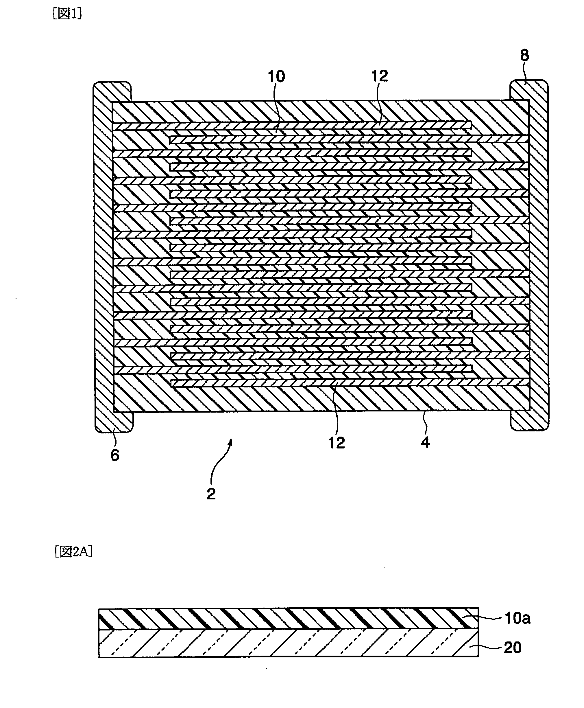
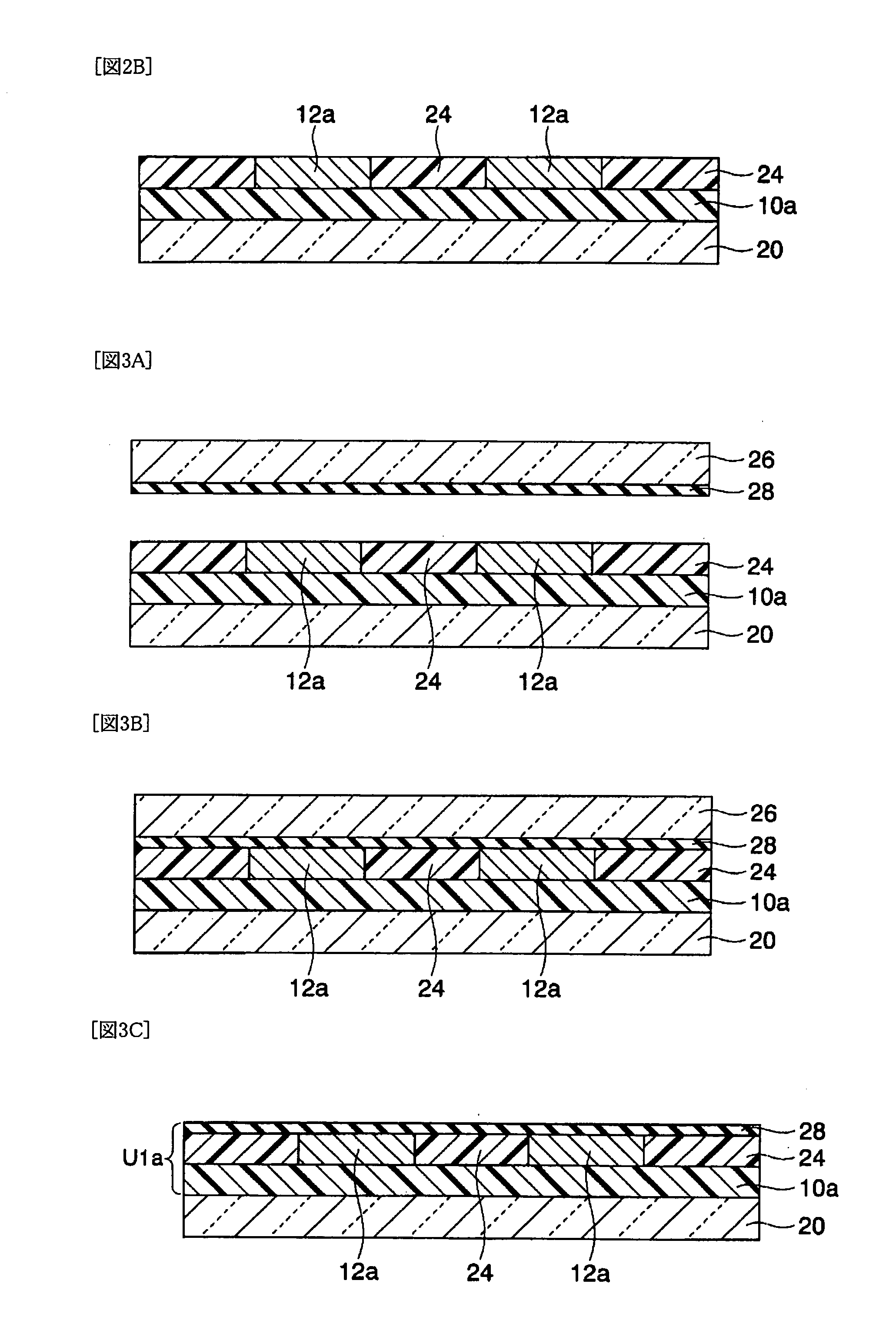
[0190] Namely, in the example 2, the adhesive layer paste was directly applied to the surface on the electrode layer side of the green sheet 10a, on which the electrode layer 12a and blank pattern 24 were formed, by using a die coater so as to form an adhesive layer.

example 3

[0198] Other than using an acrylic resin as a binder for the green sheet instead of a polyvinyl butyral resin, green chips and multilayer ceramic capacitor samples were produced in the same way as in the example 1, and the nonadhesion defect rate and short-circuiting defect rate were measured in the same way as in the example 1.

[0199] Namely, in the example 3, acrylic resin green sheet paste produced by the method below was used as green sheet paste.

[0200] Acrylic Resin Green Sheet Paste

[0201] First, an additive material mixture was produced in the same way as in the green sheet paste of the example 1. Then, the additive material mixture obtained as above in an amount of 4.3 parts by weight, ethyl acetate in an amount of 6.85 parts by weight and a dispersant in an amount of 0.04 part by weight were mixed and pulverized by using a ball mill to obtain additive slurry. The mixing and pulverizing were performed under a condition of using a 250 cc polyethylene resin container and addi...


PUM

PropertyMeasurementUnit
thicknessaaaaaaaaaa
thicknessaaaaaaaaaa
total thicknessaaaaaaaaaa

Abstract

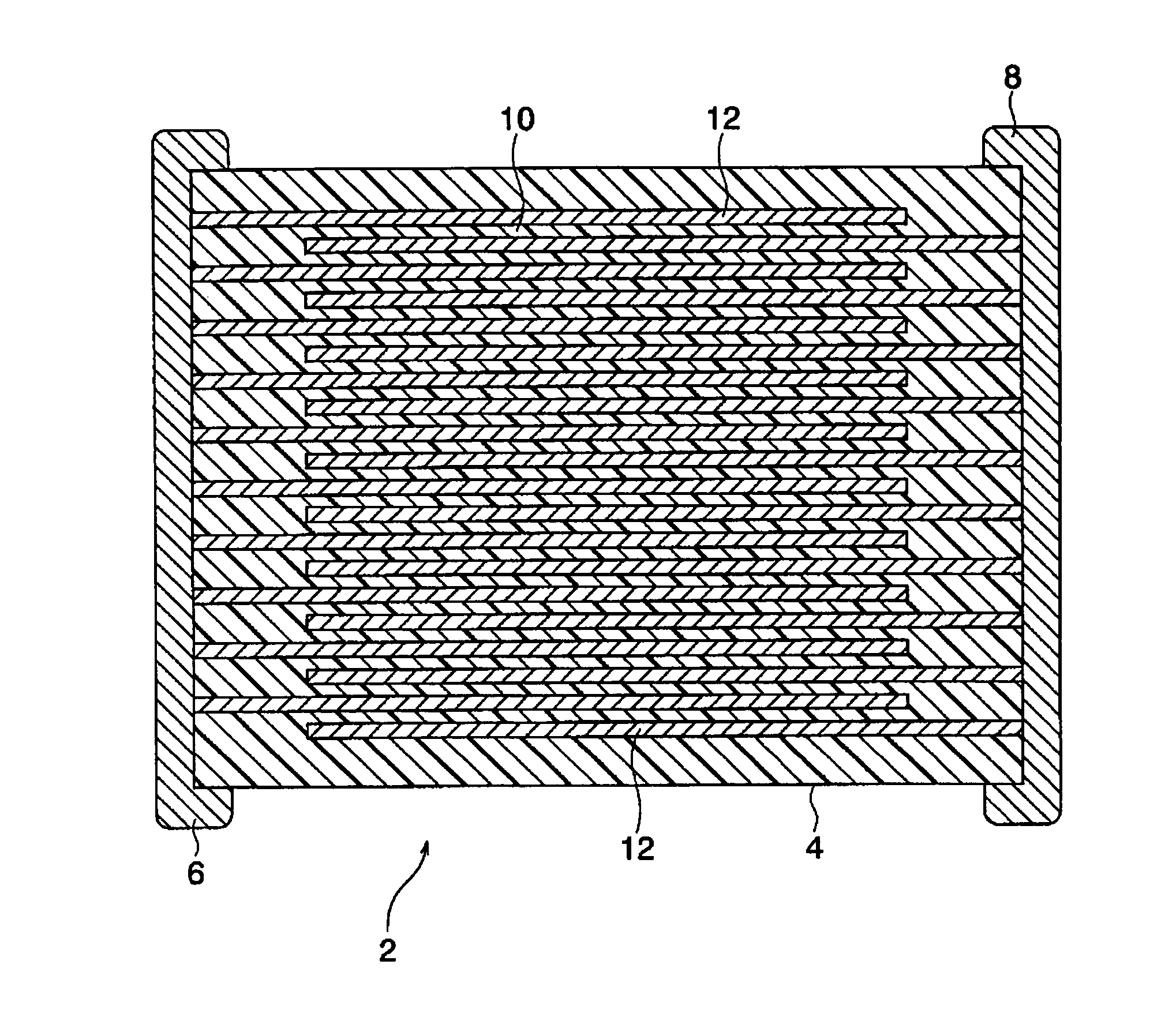
A production method of a multilayer electronic device, comprising the steps of forming a green sheet 10a; forming an electrode layer 12a on a surface of the green sheet 10a; stacking the green sheets 10a, each having the electrode layer 12a thereon, to form a green chip; and firing the green chip: wherein before stacking the green sheet 10a having the electrode layer 12a formed thereon, an adhesive layer 28 is formed on a surface on the electrode layer side of the green sheet 10a having the electrode layer 12a formed thereon; and the green sheet 10a having the electrode layer 12a formed thereon is stacked via the adhesive layer 28.

Description

TECHNICAL FIELD [0001] The present invention relates to a production method of a multilayer electronic device, such as a multilayer ceramic capacitor, and particularly relates to a production method of a low-cost multilayer electronic device having excellent stacking property (adhesiveness in stacking) and capable of reducing nonadhesion defects (nonlamination) and a short-circuiting defect rate even when a green sheet is formed to be extremely thin. BACKGROUND ART [0002] In recent years, as a result that a variety of electronic apparatuses have become more compact, electronic devices to be installed inside the electronic apparatuses have been made furthermore compact and to have higher performance. As one of the electronic devices, there is a multilayer ceramic capacitor, which has been also required to be more compact and to have higher performance. [0003] To pursue attaining of a more compact multilayer ceramic capacitor with a higher capacity, dielectric layers are strongly requ...

Claims


Application Information

Patent Timeline
Patent Type & Authority Applications(United States)
IPC IPC(8): C03B29/00
CPCH01G4/308H01G4/30
Inventor SATO, SHIGEKI
Owner TDK CORPARATION
Learn More