Semiconductor device

a technology of semiconductors and devices, applied in the direction of semiconductor devices, bulk negative resistance effect devices, electrical appliances, etc., can solve the problems of increasing the size of the memory cell, increasing the cost performance of the memory, and reducing the memory performance, so as to increase the specific resistance of the top, the specific resistance is highest, and the diameter is smallest.

a technology of semiconductors and devices, applied in the direction of semiconductor devices, bulk negative resistance effect devices, electrical appliances, etc., can solve the problems of increasing the size of the memory cell, increasing the cost performance of the memory, and reducing the memory performance, so as to increase the specific resistance of the top, the specific resistance is highest, and the diameter is smallest.

US20080054246A1Inactive Publication Date: 2008-03-06ELPIDA MEMORY INC

Image

  • Semiconductor device
  • Semiconductor device
  • Semiconductor device

Examples


Embodiment Construction

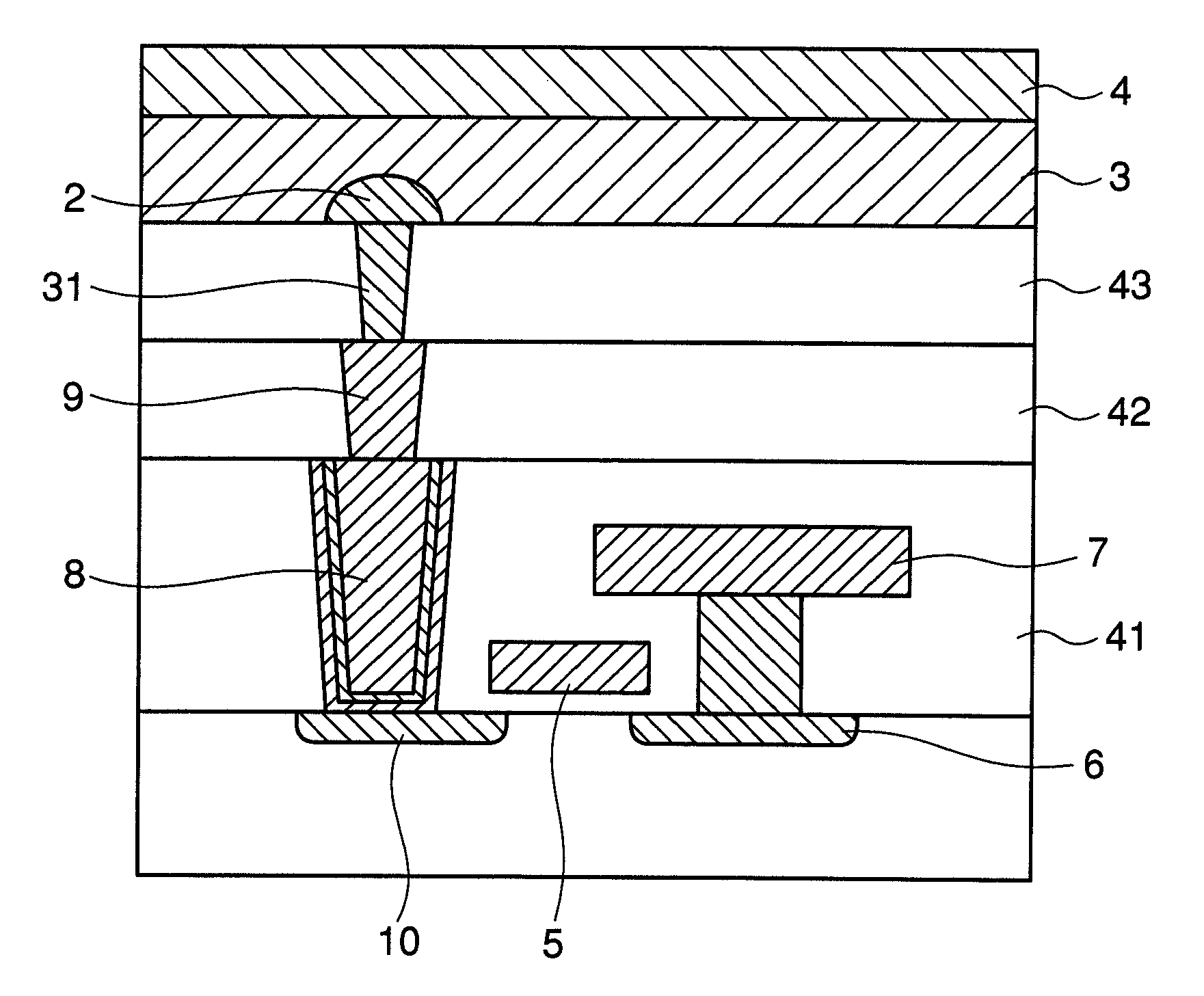
[0038]A semiconductor device according to the present invention will now be described in detail with reference to FIGS. 4 and 5. FIG. 4 is a cross-sectional view of a phase-change memory cell of the present invention. FIG. 5 is a cross-sectional view of another phase-change memory cell of the present invention. The semiconductor device of the present invention includes a buffer plug 9. Specifically, a three-stage structure composed of a heater electrode 31, the buffer plug 9, and a contact plug 8 connects between a phase-change film 3 and a drain diffusion layer 10.

[0039]The memory cell shown in FIG. 4 includes a cell transistor, a contact plug 8, a buffer plug 9, a heater electrode 31, a phase-change film 3, an upper electrode 4, and a GND wiring 7. The cell transistor is composed of a drain diffusion layer 10, a source diffusion layer 6, and a gate electrode 5. The source diffusion layer 6 is connected to the GND wiring 7 via a plug. The gate electrode 5 is connected to a word-lin...


PUM


Abstract

A semiconductor device including a contact plug connected to a diffusion layer of a cell transistor, a heater electrode connected to a phase-change film, and a buffer plug connecting between the contact plug and the heater electrode.

Description

[0001]This application is based upon and claims the benefit of priority from Japanese patent application No. 2006-241487, filed on Sep. 6, 2006, the disclosure of which is incorporated herein in its entirety by reference.BACKGROUND OF THE INVENTION[0002]1. Field of the Invention[0003]The present invention relates to a semiconductor device and more particularly to a semiconductor device including a nonvolatile memory having a phase-change film.[0004]2. Description of the Related Art[0005]Semiconductor memories used in semiconductor devices are classified into volatile memories that do not retain the stored information when the power is turned off and nonvolatile memories that can retain the stored information even when the power is turned off. Examples of the volatile memories include DRAMs (Dynamic Random Access Memories) and SRAMs (Static Random Access Memories), and examples of the nonvolatile memories include EEPROMs (Electrically Erasable Programmable Read Only Memories) and fla...

Claims


Application Information

Patent Timeline
06 Mar 2008
Publication
US20080054246A1
IPC
H01L45/00
CPC
H01L27/2436; H01L45/06; H01L45/1233; H01L45/148; H01L45/143; H01L45/144; H01L45/126; H10B63/30
Inventors
SATO, NATSUKI