High density stacked die assemblies, structures incorporated therein and methods of fabricating the assemblies

a technology of stacked dies and assembly methods, applied in the field of semiconductor devices, can solve the problems of compromising package integrity, requiring a significant amount of space or “real estate”, and significantly increasing the overall height of the die stack

Active Publication Date: 2008-03-06
MICRON TECH INC
View PDF14 Cites 38 Cited by
  • Summary
  • Abstract
  • Description
  • Claims
  • Application Information

AI Technical Summary

Problems solved by technology

One challenge posed by conventional stacked die MCM configurations is that of providing sufficient access to the bond pads of dice below the top die in a stack to enable wire bonding using conventional equipment.
While the die paddle provides alignment and support of the semiconductor die stack during assembly, the die paddle requires a significant amount of space or “real estate” and also adds significantly to the overall height of the die stack.
Further, when such a semiconductor die assembly is in operation, temperature change can create significant thermal stress between the die paddle and the adjacent semiconductor

Method used


Image

  • High density stacked die assemblies, structures incorporated therein and methods of fabricating the assemblies
  • High density stacked die assemblies, structures incorporated therein and methods of fabricating the assemblies
  • High density stacked die assemblies, structures incorporated therein and methods of fabricating the assemblies

Examples


Embodiment Construction

[0015]In the description which follows, like features and elements have been identified by the same or similar reference numerals for ease of identification and enhanced understanding of the disclosure hereof. Such identification is by way of convenience for the reader only, however, and is not limiting of the scope of the present invention or an implication that features and elements of various components and embodiments identified by like reference numerals are identical or constrained to identical functions.

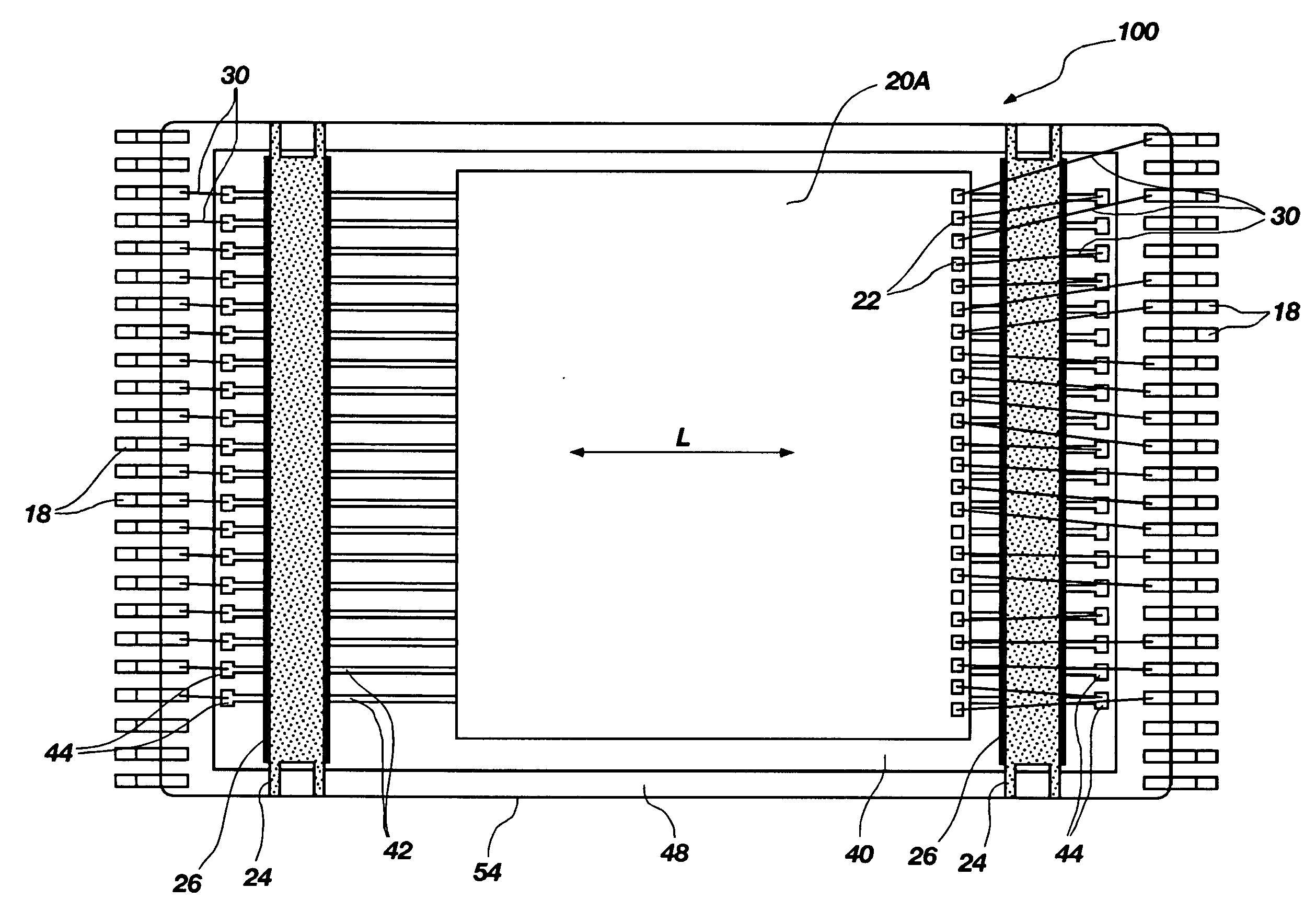
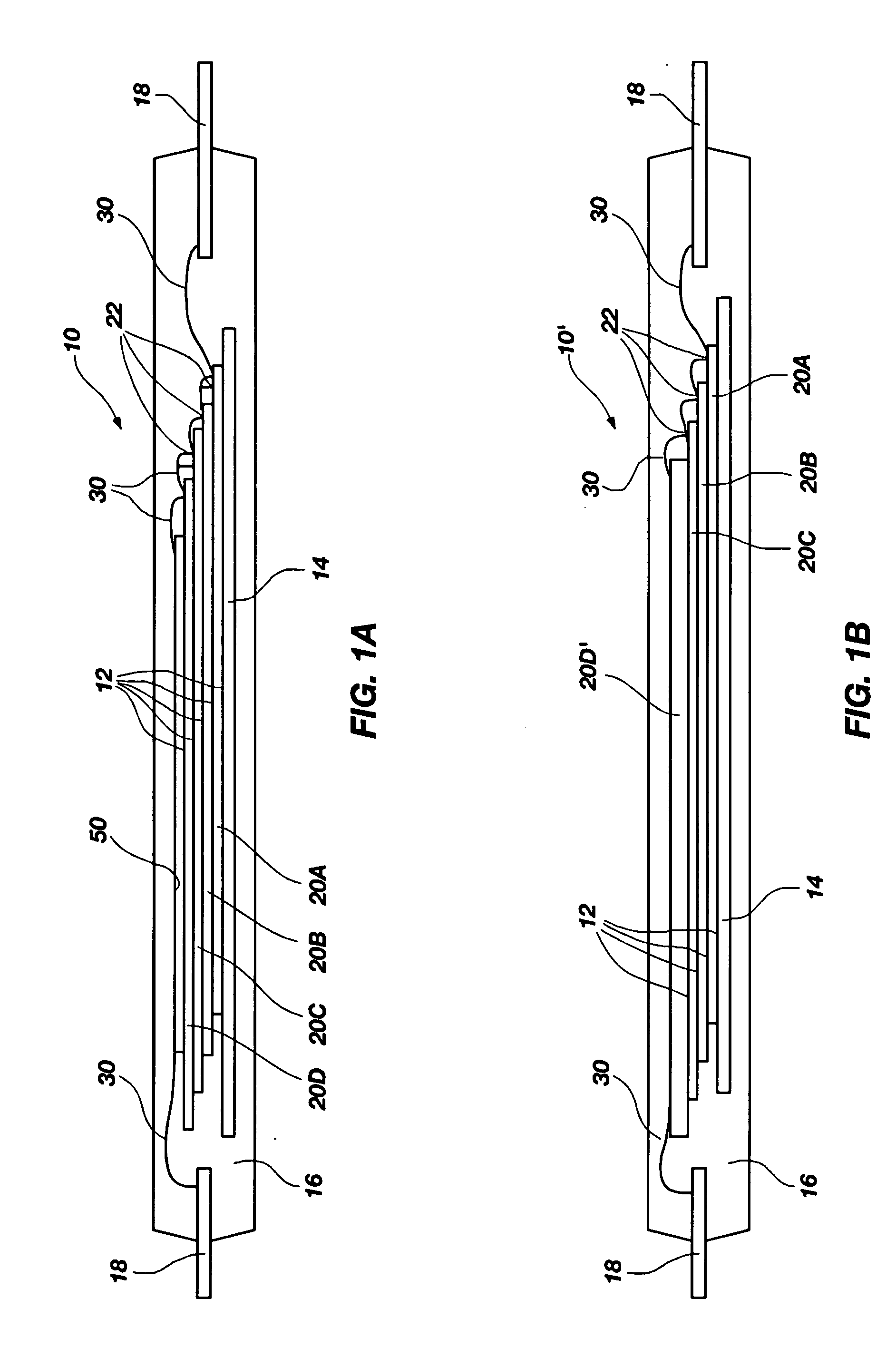
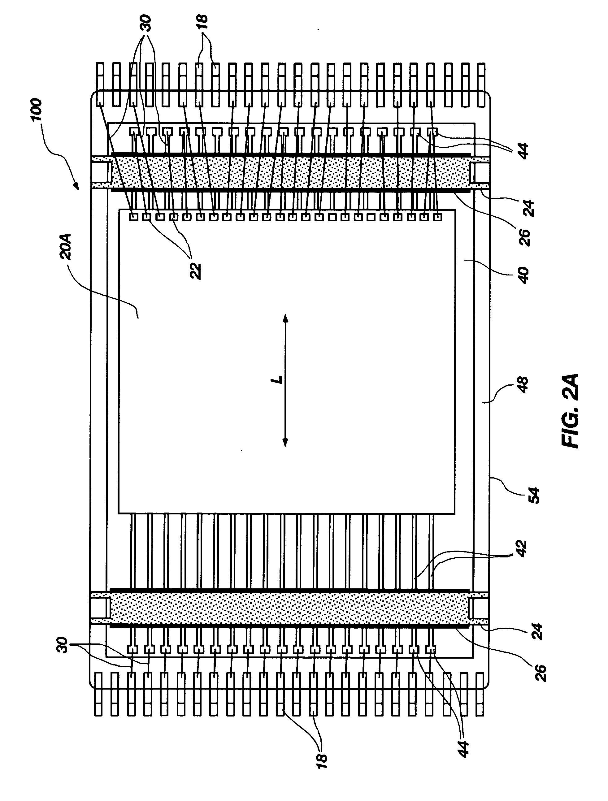
[0016]In accordance with one embodiment of the invention, a stacked multi-die assembly is formed using at least two semiconductor dice with bond pads located on one side or two adjacent sides of the individual semiconductor die, a redistribution element on which the dice are stacked comprising a substrate of semiconductor material or other material exhibiting a coefficient of thermal expansion (CTE) similar to that of the semiconductor dice, and a paddle-less lead frame having...


PUM


Abstract

A stacked semiconductor die assembly includes at least two partially offset semiconductor dice with bond pads located adjacent at least one peripheral side thereof supported on a redistribution element formed of a material of substantially similar CTE to that of the dice, and a paddle-less lead frame secured to the redistribution element during fabrication, including encapsulation. The assembly is configured to be substantially vertically symmetrical with respect to inner ends of lead fingers of the lead frame to facilitate uniform encapsulant flow. The semiconductor die assembly may be configured in a package with leads extending from two sides thereof, such as a thin small outline package (TSOP), or four sides thereof, such as a quad flat pack (QFP).

Description

BACKGROUND OF THE INVENTION[0001]Field of the Invention. Embodiments of the invention relate generally to semiconductor devices. More particularly, the invention, in various embodiments, pertains to assemblies of stacked semiconductor dice, structures incorporated in such assemblies, methods of fabricating such assemblies and systems including such assemblies.[0002]Discussion of Related Art. The use of integrated circuit (IC) chips or dice is widespread in electronics applications. Continuing progress in the manufacture of IC chips has resulted in chips of greatly increased density, i.e., a higher number of semiconductor die per footprint area of each chip. In order to produce increasingly complex electronic structures exhibiting high circuit densities, it has become common practice to stack dice on a lead frame die paddle to create what is known in the art as a multi-chip package or multi-chip module (MCM). One challenge posed by conventional stacked die MCM configurations is that ...

Claims


Application Information

Patent Timeline
IPC IPC(8): H01L23/02
CPCH01L23/49506H01L23/49531H01L2224/73265H01L2224/32145H01L24/48H01L2924/01057H01L2225/06562H01L2224/48247H01L2224/48091H01L23/49575H01L2924/00014H01L2224/48145H01L2924/00012H01L24/73H01L2924/14H01L2924/181H01L2224/05554H01L24/49H01L2224/49171H01L2224/49175H01L2924/00H01L2224/45099H01L2224/45015H01L2924/207
Inventor CORISIS, DAVID J.JIANG, TONGBILUO, SHIJIAN
Owner MICRON TECH INC
Why Eureka
Try Eureka