

Electro-optical device and electronic apparatus
a technology of electrooptical elements and electronic devices, applied in the direction of electrographic process equipment, instruments, printing, etc., can solve the problems of large circuit size, difficulty in reducing the size of the first and second signal processing circuits, and inability to generate such a small current with high precision and implement correction over a wide rang
- Summary
- Abstract
- Description
- Claims
- Application Information
AI Technical Summary
Benefits of technology
Problems solved by technology
Method used
Image

Examples
first embodiment
A. First Embodiment
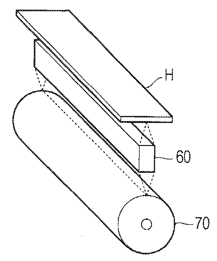
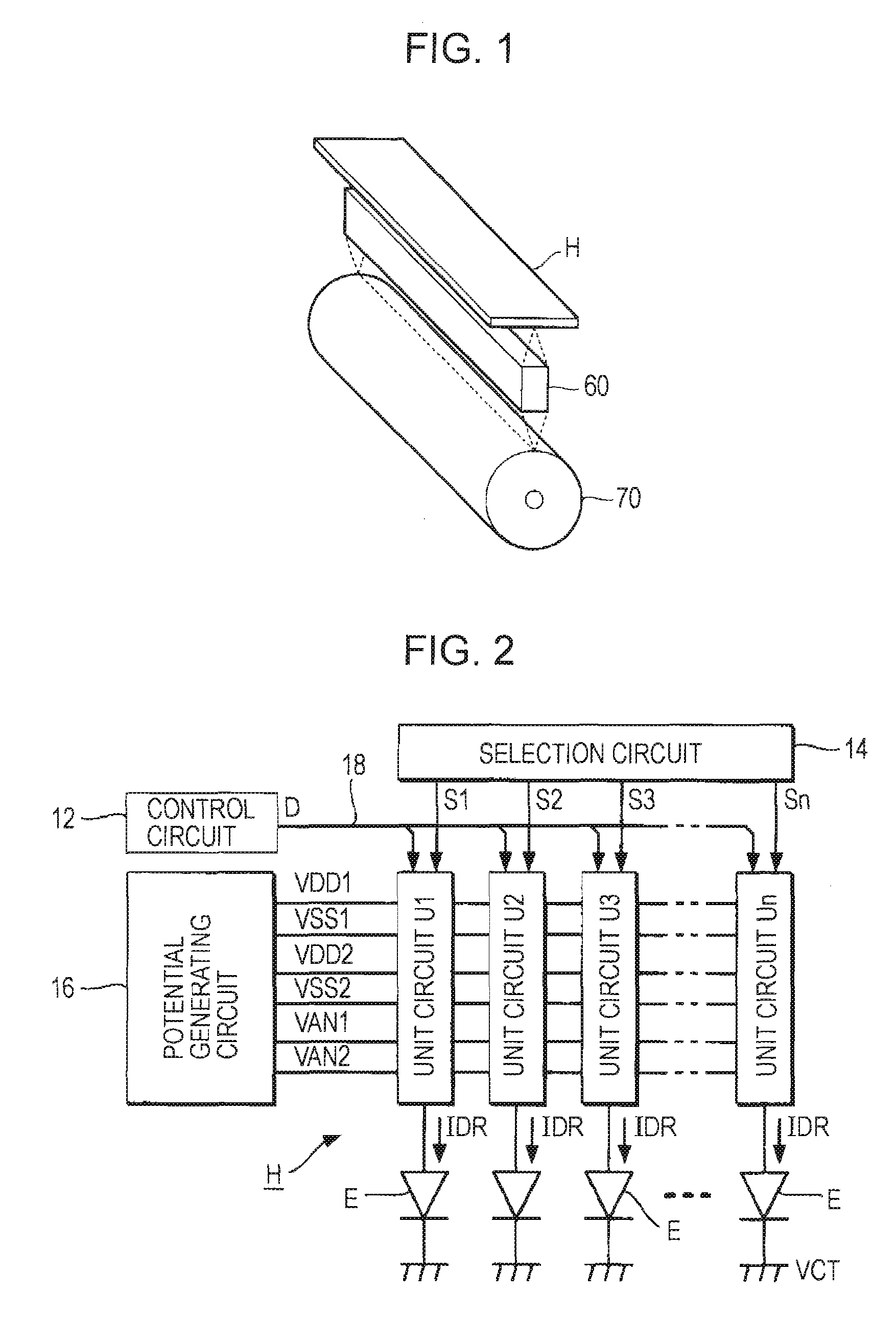
[0034]FIG. 1 is a perspective view of the structure of part of an electrophotographic image forming apparatus using an electro-optical device according to a first embodiment of the invention as an exposure device (line head). As shown in FIG. 1, the image forming apparatus includes an electro-optical device H, a converging lens array 60, and a photosensitive drum 70. The photosensitive drum 70 is supported by a rotating shaft extending in a main scanning direction and rotates in such a manner that the peripheral surface of the photosensitive drum 70 faces the electro-optical device H. The converging lens array 60 is a condenser having an array of many gradient index lenses and is positioned between the electro-optical device H and the photosensitive drum 70.
[0035]FIG. 2 is a block diagram of the structure of the electro-optical device H. As shown in FIG. 2, the electro-optical device H includes an array of n electro-optical elements E arranged in the main scanning...
second embodiment
B. Second Embodiment
[0053]Next, a second embodiment of the invention will be described. The elements of the second embodiment with operations and functions common to those of the first embodiment are denoted with the same reference numerals, and detailed descriptions thereof are omitted where appropriate.
[0054]FIG. 8 is a block diagram of the structure of the unit circuit Ui, As shown in FIG. 8, the unit circuit Ui according to the second embodiment additionally includes, besides the elements of the unit circuit Ui according to the first embodiment (FIG. 5), a selection circuit 21 positioned between an output end of the memory M1 and the gate of the current source Q1, and a selection circuit 22 positioned between an output end of the memory M2 and the gate of the current source Q2. The potential generating circuit 16 additionally generates, besides the potentials shown in FIG. 4, potentials VG1 and VG2. The potential VG1 is a potential greater than or equal to the potential VSS1 and...
third embodiment
C. Third Embodiment
[0058]The number of signal processing circuits C or the number of current sources Q included in one unit circuit Ui is not limited to that in the above examples. For example, as shown in FIG. 9, the structure of one unit circuit Ui having three signal processing circuits C (C1 to C3) and three current sources Q (Q1 to Q3) may be adopted. The current source Q3 is a p-channel thin-film transistor generating a correction current I3 according to the voltage between the gate and the source of the current source Q3 and supplying the correction current I3 to the node z.
[0059]FIG. 10 is a conceptual diagram showing the level of each potential generated by the potential generating circuit 16. As shown in FIG. 10, the potential generating circuit 16 according to a third embodiment additionally generates, besides the potentials shown in FIG. 4, three types of potentials (VDD3, VSS3, and VAN3). The potential VDD3 is the same potential as the potential VDD2. The potential VAN3...
PUM
 Abstract
Description
Claims
Application Information