Inspection apparatus and method

a technology of inspection apparatus and inspection method, which is applied in the direction of optical radiation measurement, material analysis using wave/particle radiation, instruments, etc., can solve the problems of difficult surface detection, long inspection time, and difficulty in detecting the surface of an insulator using a secondary electron beam, etc., and achieves the effect of high resolution and lengthening inspection tim

Inactive Publication Date: 2008-03-13
NEC ELECTRONICS CORP
View PDF4 Cites 16 Cited by
  • Summary
  • Abstract
  • Description
  • Claims
  • Application Information

AI Technical Summary

Benefits of technology

[0018] With the inspection apparatus of Patent Document 1, it is necessary to narrow down the electron beam in a case where a high resolution is obtained. This lengthens inspection time.

Problems solved by technology

This lengthens inspection time.
However, it is thought that detecting the surface, etc., of an insulator using a secondary electron beam is difficult to perform owing to charge-up, etc.
Accordingly, problems remain in terms of implementing an inspection apparatus, particularly a wafer inspection apparatus, that is capable of delivering higher resolution and higher speed.

Method used


Image

  • Inspection apparatus and method
  • Inspection apparatus and method
  • Inspection apparatus and method

Examples


Embodiment Construction

OF THE INVENTION

[0039] The present invention will be described in detail with reference to the accompanying drawings.

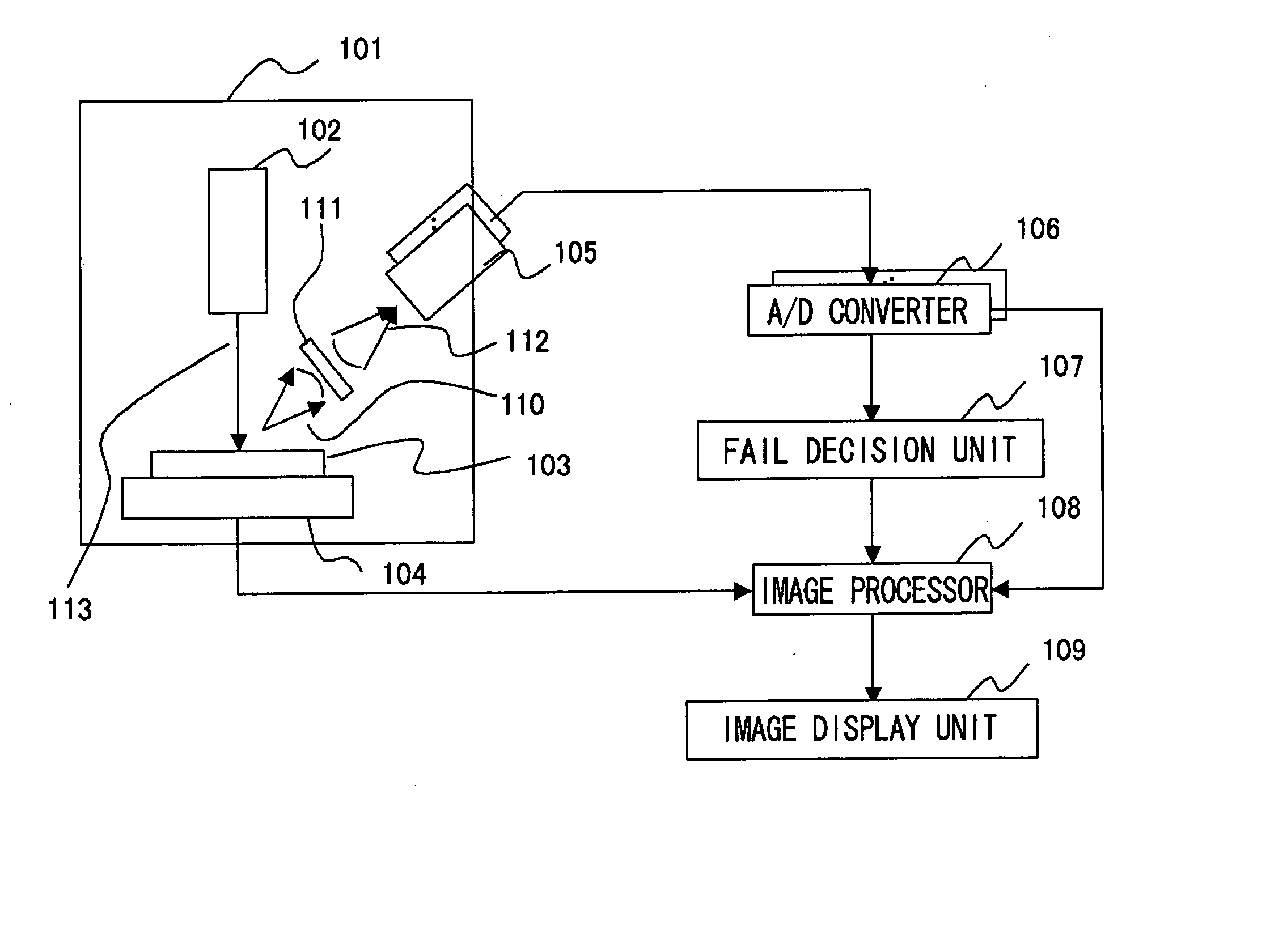
[0040]FIG. 1 is a diagram illustrating the configuration of an example of the present invention. As shown in FIG. 1, a sample (DUT) (103) under inspection is area-irradiated with an excitation beam. X-rays (110) from the sample (103) are converged by a high-resolution X-ray lens (zone plate) (111) and an image is formed on a detector (105). The detection signal from the detector (105) is converted to a digital signal by an A / D converter (106) and pass / fail is decided by a fail decision unit (107). If a fail is found, image processing is executed by an image processor (108) and the processed image is displayed on an image display unit (109). According to the present invention, the sample (103) is area-irradiated with an electron beam serving as the excitation beam. X-rays (110) from the sample are fluorescent X-rays from the area of the sample that have been area-irra...


PUM

PropertyMeasurementUnit
widthaaaaaaaaaa
sizeaaaaaaaaaa
angleaaaaaaaaaa

Abstract

Provided is an apparatus for acquiring information about the interior of a sample non-destructively and with high resolution, determining pass/fail of the sample and shortening inspection time. A sample is irradiated with an electron beam or X-rays, fluorescent X-rays from the sample are converted using a zone plate and are detected by a detector, an electric signal from the detector is converted to a digital signal by an A/D converter and the digital signal is applied to a fail decision unit, which determines pass/fail of the sample. If the sample is fail, an image processor applies image processing and presents a display on an image display unit.

Description

FIELD OF THE INVENTION [0001] This invention relates to an inspection technique and, more particularly, to an inspection apparatus and method ideal for application to non-destructive and non-contact defect inspection of semiconductor devices. BACKGROUND OF THE INVENTION [0002] An example of a non-destructive and non-contact inspection apparatus of this kind is disclosed in Patent Document 1. The disclosed apparatus includes means for irradiating a sample (a semiconductor device) with an electron beam and detecting the intensity of characteristic X-rays dependent upon the amount of a specific substance present at the position irradiated with the electron beam, and monitor means for monitoring the X-ray intensity detected. The apparatus further includes decision means for deciding failure based upon the value of X-ray intensity detected. When failure has been decided by the monitor means, the location of the defect is displayed on a display unit. According to the apparatus and method ...

Claims


Application Information

Patent Timeline
Patent Type & Authority Applications(United States)
IPC IPC(8): G01N23/223G01J1/42G01N23/225
CPCH01J2237/2561G01N23/2252
Inventor NAKAMURA, TOYOKAZU
Owner NEC ELECTRONICS CORP
Why Eureka
Try Eureka