Reconfigurable semiconductor intergrated circuit and processing assignment method for the same

a technology processing assignments, which is applied in the direction of computation using denominational number representation, pulse techniques, instruments, etc., can solve the problems of insufficient or excessive performance of reconfigurable semiconductor integrated circuits, clock skews that must be readjusted over the entire existing circuit, and require redesign, so as to achieve the effect of shortening the design time of a new reconfigurable semiconductor integrated circui

Inactive Publication Date: 2008-03-13
SOCIONEXT INC
View PDF5 Cites 19 Cited by
  • Summary
  • Abstract
  • Description
  • Claims
  • Application Information

AI Technical Summary

Benefits of technology

[0035] As described above, according to the present invention, even if there arises a necessity to redesign a reconfigurable semiconductor integrated circuit, no clock redesign involving existing circuits is necessary. Thus, the design time of a new reconfigurable semiconductor integrated circuit can be effectively shortened.

Problems solved by technology

Even in a reconfigurable semiconductor integrated circuit, there may arise a necessity to redesign the reconfigurable semiconductor integrated circuit itself in such a case that the performance thereof is insufficient or excessive for a required processing amount, for example.
For this reason, clock skew must be readjusted over the entire existing circuits, and this requires redesign.
This drawback also applies to the case of deleting an unnecessary circuit.
Conventionally, therefore, if there arises a necessity to redesign the reconfigurable semiconductor integrated circuit, it is unable to satisfy the demand for shortening the design time effectively.

Method used


Image

  • Reconfigurable semiconductor intergrated circuit and processing assignment method for the same
  • Reconfigurable semiconductor intergrated circuit and processing assignment method for the same
  • Reconfigurable semiconductor intergrated circuit and processing assignment method for the same

Examples


embodiment 1

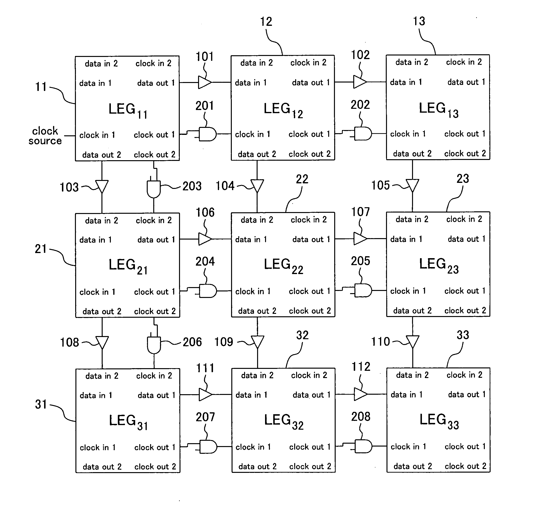
[0056]FIG. 1 is a view showing a configuration of a reconfigurable semiconductor integrated circuit of Embodiment 1 of the present invention.

[0057] The reconfigurable semiconductor integrated circuit of FIG. 1 has nine logic element groups 11 to 13, 21 to 23 and 31 to 33 arranged in a two-dimensional matrix of three rows and three columns (M×N=3×3). Each of the logic element groups 11 to 33 includes at least one logic element (not shown). Each logic element is provided with a plurality of operators, a plurality of resistors, memories and the like although not shown. Each of the logic element groups 11 to 33 also includes two clock input terminals clock in 1 and clock in 2, two clock output terminals clock out 1 and clock out 2, two data input terminals data in 1 and data in 2, and two data output terminals data out 1 and data out 2. Note that at least one of each kind of these terminals may be provided.

[0058] Supply of a clock signal to the reconfigurable semiconductor integrated ...

embodiment 2

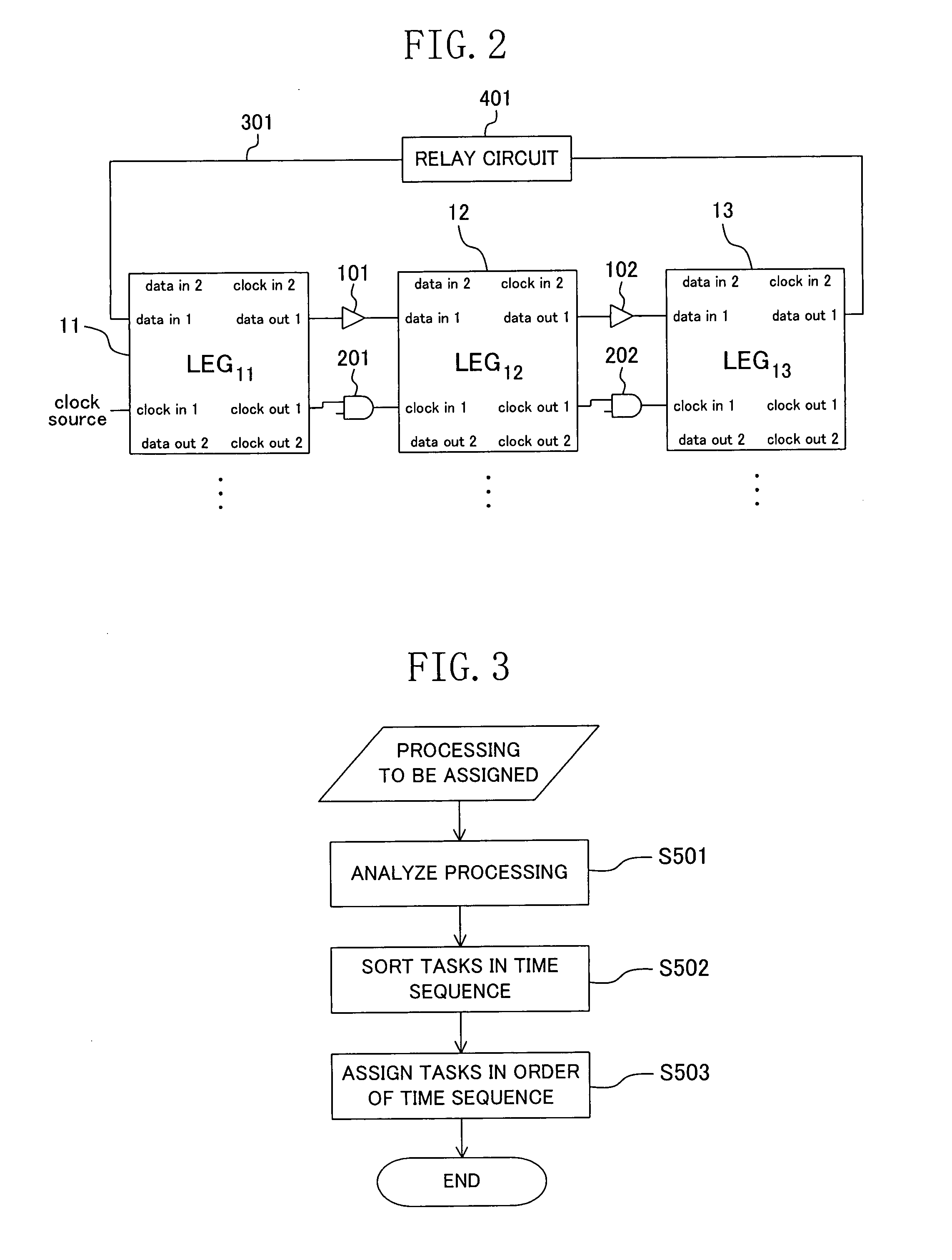
[0088]FIG. 7 shows a schematic configuration of a reconfigurable semiconductor integrated circuit of Embodiment 2 of the present invention.

[0089] In FIG. 7, the reconfigurable semiconductor integrated circuit of this embodiment is identical to that of Embodiment 1 shown in FIG. 1 except for clock line routing.

[0090] In this embodiment, the clock line is routed as follows. A skew-adjusted clock signal is inputted into the three logic element groups 11 to 13 on the first row. Clock signals outputted from the logic element groups 11 to 13 are skew-adjusted and inputted into the logic element groups 21 to 23 on the second row, and clock signals outputted from the logic element groups 21 to 23 are skew-adjusted and inputted into the logic element groups 31 to 33 on the third row.

[0091] In Embodiment 1, clock skew is not made uniform among the logic element groups 11 to 33. In this embodiment, clock skew is made uniform for the logic element groups on the same row.

[0092] Accordingly, ...

embodiment 3

[0100]FIG. 9 shows a configuration of a reconfigurable semiconductor integrated circuit of Embodiment 3 of the present invention.

[0101] The reconfigurable semiconductor integrated circuit of this embodiment is identical to that of Embodiment 1 except for clock line routing.

[0102] In this embodiment, in the logic element groups 11 to 33 arranged in a two-dimensional matrix of three rows and three columns (x=3, y=3), the clock line is first routed to the first-row, first-column logic element group 11. Thereafter, the clock line is routed to the first-row, second-column logic element group 12 and the second-row, first-column logic element group 21, then to the first-row, third-column logic element group 13, the second-row, second-column logic element group 22 and the third-row, first-column logic element group 31, then to the second-row, third-column logic element group 23 and the third-row, second-column logic element group 32, and finally to the third-row, third-column logic elemen...


PUM


Abstract

A plurality of logic element groups LEG11 to LEG33 respectively include at least one logic element as a component of a reconfigurable semiconductor integrated circuit. Between any logic element groups engaging in data transmission/reception, e.g., LEG11 and LEG12, clock out terminal and clock in terminal are connected via a line while data out terminal and data in terminal are connected via a delay element 101. The logic element groups LEG11 to LEG33 are therefore independent of one another in terms of timing design. Thus, if redesign is necessary for a semiconductor integrated circuit completed with a plurality of logic element groups, only a new circuit may be designed and connected to an existing circuit, or an unnecessary logic element group may just be removed, to complete a new semiconductor integrated circuit.

Description

TECHNICAL FIELD [0001] The present invention relates to a reconfigurable semiconductor integrated circuit and a processing assignment method for the same. BACKGROUND ART [0002] In recent years, with improvement in the degree of semiconductor integration, a system integrated into LSI has become larger in scale and more complicated. As a result, the design time has increased, and also the incidence of unavoidable design defects in software has increased. In the market, however, demands have been made for further reduction in turnaround time (TAT) (shortening of the design time of a new product) and higher quality design. [0003] To address the above problem, there is known a technology in which a reconfigurable semiconductor integrated circuit is used to contribute to shortening of the design time and reduction in the number of defects. A reconfigurable semiconductor integrated circuit includes programmable logic devices represented by recently available field programmable gate arrays ...

Claims


Application Information

Patent Timeline
Patent Type & Authority Applications(United States)
IPC IPC(8): H03K19/00
CPCH03K19/1774G06F17/5054G06F30/34
Inventor TETSUKAWA, TATSUYAOKAMOTO, MINORUMARUI, SHINICHI
Owner SOCIONEXT INC
Why Eureka
Try Eureka