Semiconductor device having pseudo power supply wiring and method of designing the same

a technology of power supply wiring and semiconductor devices, which is applied in the direction of cad circuit design, semiconductor/solid-state device details, instruments, etc., can solve the problems of difficult determination of whether the source of the transistor that constitutes the circuit block is connected to the main power supply wiring or the pseudo power supply wiring, and the sub-threshold current of a transistor in an off state increases, so as to reduce the design cost and facilitate modification. , the effect of mask defect analysis

Inactive Publication Date: 2008-03-20
ELPIDA MEMORY INC
View PDF4 Cites 1 Cited by
  • Summary
  • Abstract
  • Description
  • Claims
  • Application Information

AI Technical Summary

Benefits of technology

[0028]Because the connection destination of the source is switched easily even though improper connections are found or logical changes are required, a mask is modified

Problems solved by technology

Thus, there occurs a problem in that a sub-threshold current of a transistor in an off state increases.
However, if the logic of the circuit block is complicated, verification of the logic fixed at the time of standby state is also complicated.
Namely, determination as to whether the source of the transistor that constitutes the circuit block is connected to the main power supply wiring or the pseudo power supply wiring is difficult.
If the sourc

Method used


Image

  • Semiconductor device having pseudo power supply wiring and method of designing the same
  • Semiconductor device having pseudo power supply wiring and method of designing the same
  • Semiconductor device having pseudo power supply wiring and method of designing the same

Examples


Embodiment Construction

[0044]Preferred embodiments of the present invention will now be explained in detail with reference to the drawings.

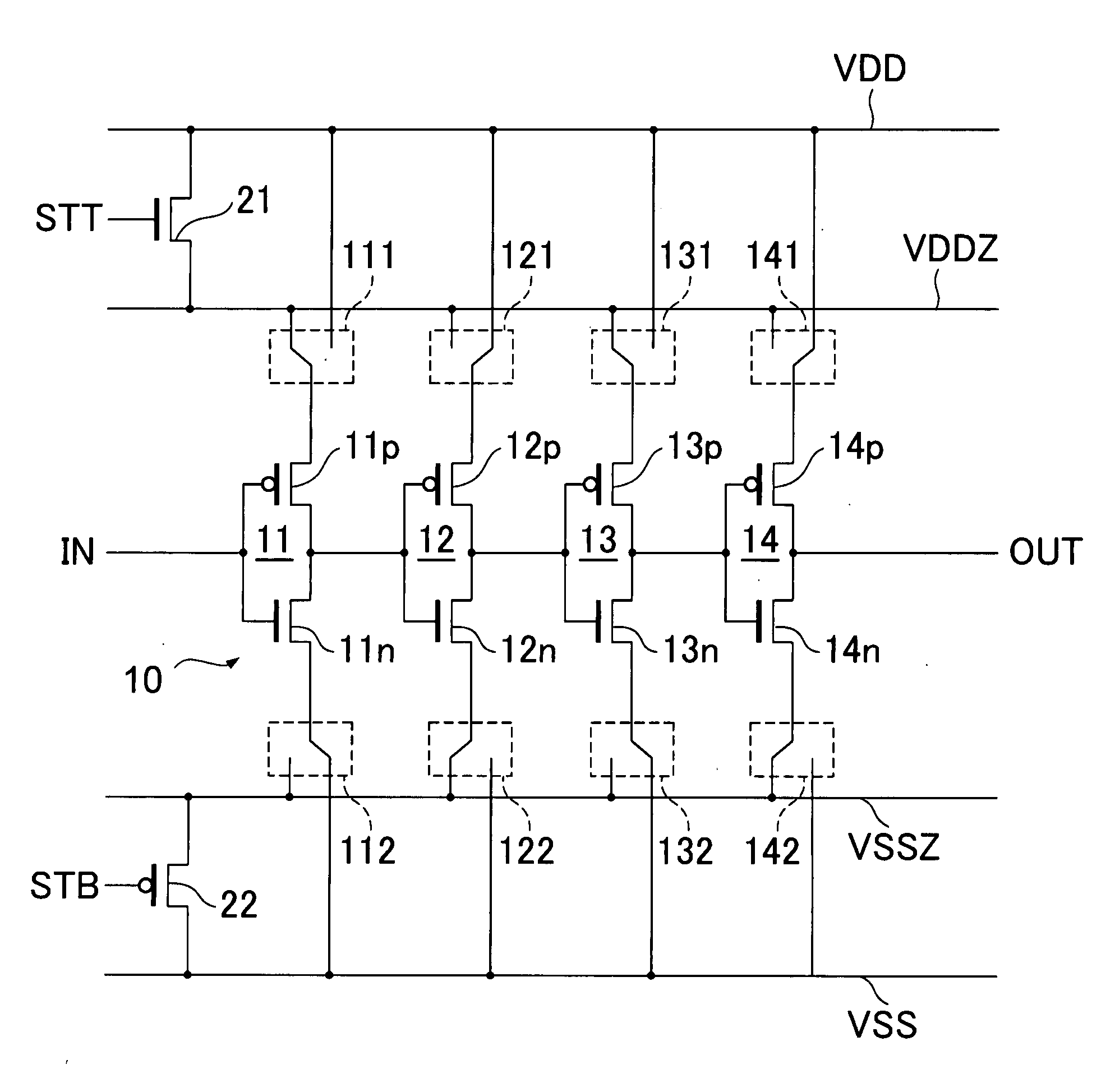
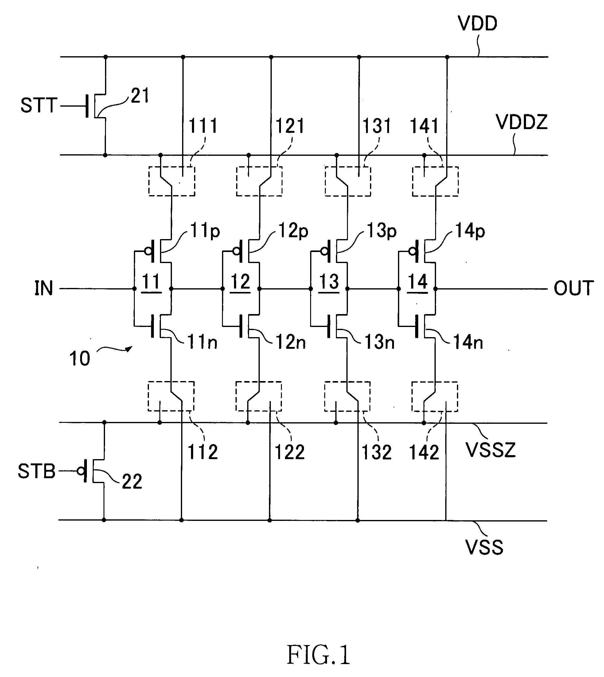
[0045]FIG. 1 is a circuit diagram conceptually showing characteristics of a semiconductor device according to a preferred embodiment of the present invention.

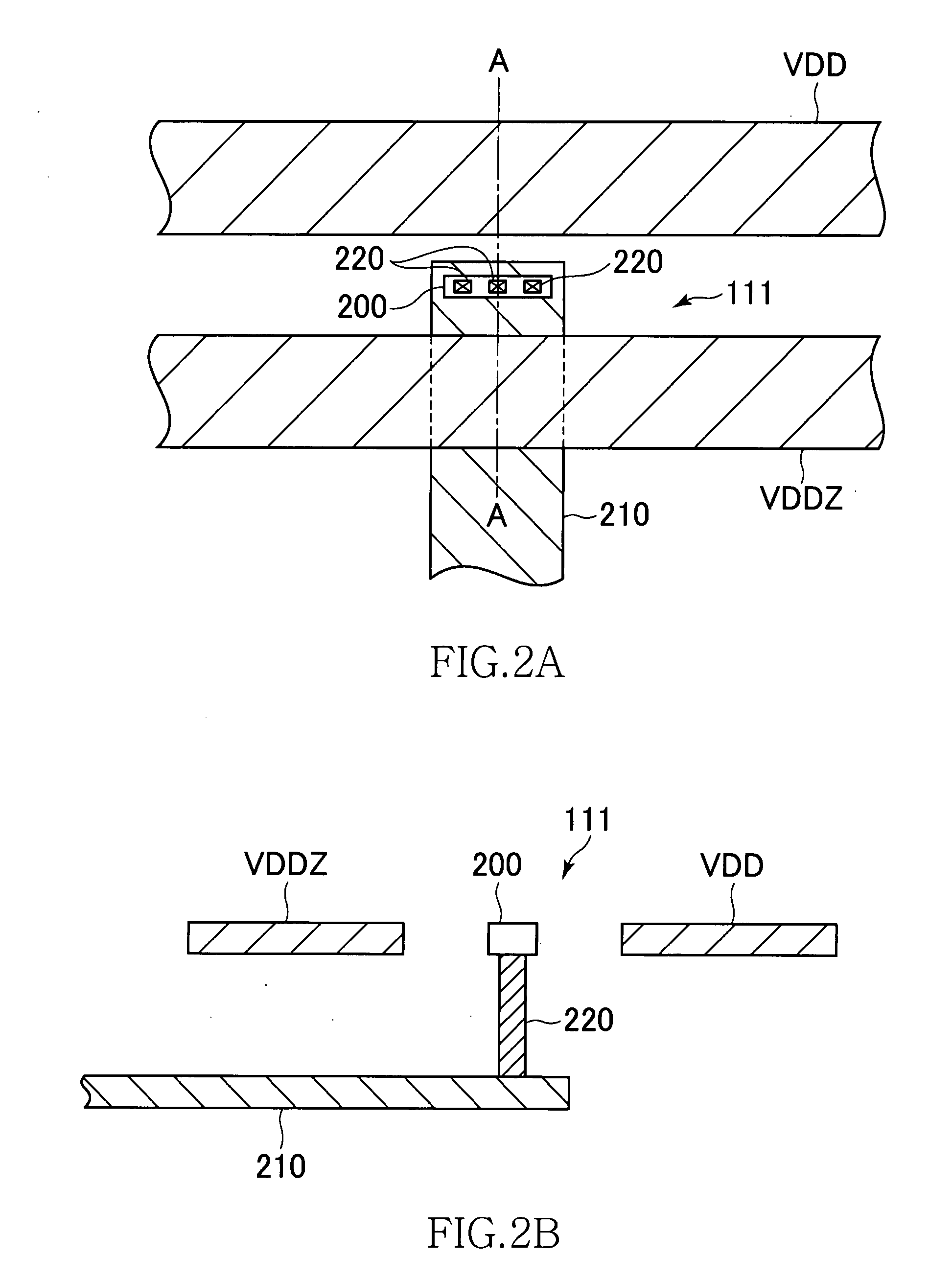
[0046]As shown in FIG. 1, the circuit configuration of the semiconductor device according to the present embodiment is the same as that of FIG. 10. Among four circuit inverters 11 to 14 included in the circuit block 10, the first inverter 11 and the third inverter 13 are connected between the pseudo power supply wiring VDDZ and the main power supply wiring VSS. The second inverter 12 and the fourth inverter 14 are connected between the main power supply wiring VDD and the pseudo power supply wiring VSSZ. The N-channel MOS transistor 21 is provided between the main power supply wiring VDD and the pseudo power supply wiring VDDZ and its gate electrode receives the standby signal STT. The P-channel MOS transistor 22 ...


PUM


Abstract

Inverters are connected between a pseudo power supply wiring and a main power supply wiring, while inverters are connected between a main power supply wiring VDD and a pseudo power supply wiring. Connected to the sources of transistors are switching areas for switching to the main power supply wiring or the pseudo power supply wiring. Connected to the sources of transistors are switching areas for switching to the main power supply wiring or the pseudo power supply wiring. Even if improper connections are found or logical changes are required, the connection destination of the source is switched easily.

Description

TECHNICAL FIELD[0001]The present invention relates to a semiconductor device and a method of designing the same, and, more particularly to a semiconductor device that has a pseudo power supply wiring for reducing standby power consumption and a method of designing the same.BACKGROUND OF THE INVENTION[0002]In recent years, an operating voltage of a semiconductor device is gradually decreasing for the purposes of reducing consumption power, and at present, a very low voltage of as low as 1 bolt is sometimes used. When the operating voltage decreases, a threshold voltage of a transistor needs to be decreased. Thus, there occurs a problem in that a sub-threshold current of a transistor in an off state increases. To solve such a problem, a method of dividing a power supply wiring into a main power supply wiring and a pseudo power supply wiring is proposed in Japanese Patent Application Laid-open Nos. 2000-13215 and 2000-48568.[0003]FIG. 10 is a circuit diagram of a general semiconductor ...

Claims


Application Information

Patent Timeline
IPC IPC(8): H01L27/105G06F17/50
CPCG06F17/5068G06F2217/78H01L23/5286H01L27/0207H01L2924/0002H01L2924/00G06F30/39G06F2119/06
Inventor RIHO, YOSHIROOTA, KENNODA, HIROMASAMIYATAKE, SHINICHI
Owner ELPIDA MEMORY INC
Why Eureka
Try Eureka