[0018]The potential of the electric supply line does not have to be always almost constant. That is, it is enough that the potential of the electric supply line is maintained at an almost constant level while the switching element is in the on-state. In the other periods, it does not matter that the potential of the electric supply line varies or is almost constant. Further, the term “almost constant” not only means a state of substantial constant but also allows a certain range of variation as long as the
advantage of the invention can be accomplished even in the presence of the variation in the range. That is, during the period in which the third switching element is in the on-state, although the potential of the electric supply line varies in a range from a first potential to a second potential, a difference between levels of gray scale displayed by the electro-optical element at the first potential and at the second potential does not cause any troubles in practical use (for example, when the electro-optical element is used as a
display device and the difference between the levels of gray scale at the first potential and the second potential cannot be sensed by a user), potentials in the range from the first potential to the second potential can be referred to as the “almost constant” potential.
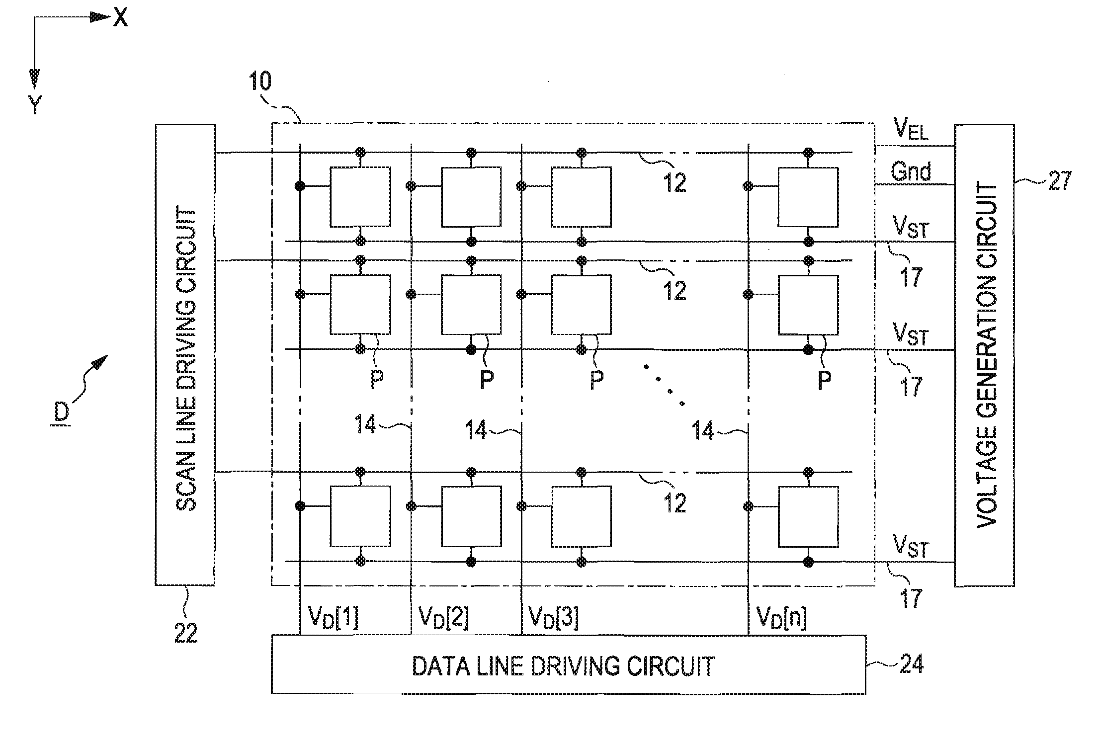
[0019]According to further aspect of the invention, there is provided an electro-optical device, comprising a plurality of data lines, a plurality of scan lines, an electric supply line, and a plurality of unit circuits disposed to correspond to respective intersections of the plurality of data lines and the plurality of scan lines, where each of plurality of the data lines is supplied with a data potential corresponding to a level of gray scale, each of the plurality of scan lines is supplied with a scan
signal which defines a writing period in which the data potential is loaded into the corresponding unit circuit, and the electric supply line is supplied with a predetermined potential, in which each of the plurality of unit circuits includes a drive transistor for generating a driving current corresponding to a potential of a gate thereof, an electro-optical element displaying a level of gray scale corresponding to the driving current, a first switching element for controlling
electrical connection and disconnection between the gate and a drain of the drive transistor, a capacitive element having a first electrode and a second electrode, a second switching element for controlling
electrical connection and disconnection between each of the plurality of data lines and the first electrode on the basis of the scan signal, a third switching element which is a switching element for controlling electrical connection and disconnection between the electric supply line and the first electrode, which is in an on-state when the second switching element is in an off-state, and which is in the off-state when the second switching element is in the on-state, and a fourth switching element interposed between the first electrode and the second electrode for controlling electrical connection and disconnection between the first electrode and the second electrode, where the second electrode is connected to the gate of the drive transistor and the electric supply line extends in a direction so as not to intersect the
scan line.
[0020]In other words, the electro-optical device includes a plurality of data lines, a plurality of scan lines, an electric supply line, and a plurality of unit circuits disposed to correspond to respective intersections of the plurality of data lines and the plurality of scan lines, where each of plurality of the data lines is supplied with a data potential corresponding to a level of gray scale, each of the plurality of scan lines is supplied with a scan signal which defines a writing period in which the data potential is loaded into the corresponding unit circuit, and the electric supply line is supplied with a predetermined potential, in which each of the plurality of unit circuits includes a drive transistor for generating a driving current corresponding to a potential of a gate thereof, an electro-optical element displaying a level of gray scale corresponding to the driving current, a first switching element for controlling electrical connection and disconnection between the gate and a drain of the drive transistor, a capacitive element having a first electrode and a second electrode, a second switching element for controlling electrical connection and disconnection between each of the plurality of data lines and the first electrode on the basis of the scan signal, a third switching element which is a switching element for controlling electrical connection and disconnection between the electric supply line and the first electrode, which is in an on-state when the second switching element is in an off-state, and which is in the off-state when the second switching element is in the on-state, and a fourth switching element interposed between the first electrode and the second electrode for controlling electrical connection and disconnection between the first electrode and the second electrode, where the second electrode is connected to the gate of the drive transistor and the electric supply line is arranged in parallel with the
scan line.
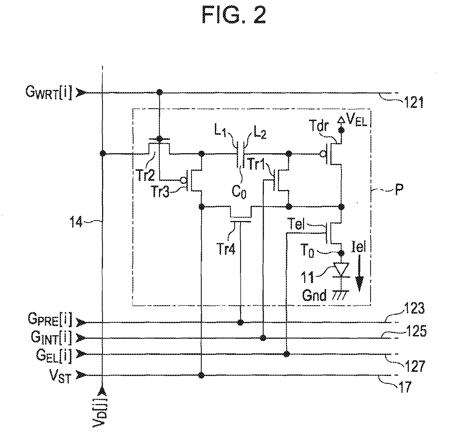
[0021]According to still further aspect of the invention, there is provided an optical device comprising a plurality of data lines, a plurality of scan lines, a plurality of electric supply lines, and a plurality of unit circuits disposed to correspond to respective intersections of the plurality of data lines and the plurality of scan lines, where each of plurality of the data lines is supplied with a data potential corresponding to a level of gray scale, each of the plurality of scan lines is supplied with a scan signal which defines a writing period in which the data potential is loaded into the corresponding unit circuit and the electric supply line is supplied with a predetermined potential, in which each of the plurality of unit circuits includes a drive transistor for generating a driving current corresponding to a potential of a gate thereof, an electro-optical element displaying a level of gray scale corresponding to the driving current, a first switching element (for example, transistor Tr1 in FIG. 2) for controlling electrical connection and disconnection between the gate and a drain of the drive transistor, a capacitive element having a first electrode and a second electrode connected to the gate of the drive transistor, a second switching element (for example, transistor Tr2 in FIG. 2) for controlling electrical connection and disconnection between the data lines and the first electrode on the basis of the scan signal, a third switching element (for example, transistor Tr3 in FIG. 2) which is a switching element for controlling electrical connection and disconnection between the electric supply line and the first electrode, which is in an on-state when the second switching element is in an off-state, and which is in the off-state when the second switching element is in the on-state, and a fourth switching element interposed between the first electrode and the second electrode for controlling electrical connection and disconnection between the first electrode and the second electrode, where the electric supply line is arranged in parallel with the scan line.
[0022]In the electro-optical device according to this aspect, it is preferable that after the fourth switching element is turned on a reset period (for example, period Pa in FIG. 4), the first switching element is turned on in a first period (for example, compensation period Pb in FIG. 4), the second switching element is turned on and simultaneously the third switching element is turned off in a second period (for example, writing period PWRT in FIG. 4) which is the succeeding period of the first period, and the second switching element is turned off and simultaneously the third switching element is turned on in a third period (for example, light-emitting period PEL in FIG. 4) which is the succeeding period of the second period. The capacitive element according to this aspect serves as a
coupling capacitor which changes the potential of the gate of the drive transistor to a potential corresponding to the data potential and also serves as a storage
capacitor for maintaining the gate of the drive transistor at a predetermined potential during the third period.
[0023]In the electro-optical device according to this aspect, it is preferable that the electric supply line is formed of a wiring layer which is the same layer as used for forming the gate of the drive transistor. With such a configuration, it is possible to form the electric supply line and the gate of the drive transistor by the same process and thus it is possible to form the electric supply line without forming an additional wiring layer.

