Apparatus and methods for the inspection of microvias in printed circuit boards

a printed circuit board and micro-via technology, applied in the field of micro-via inspection apparatus and printed circuit board scanning and imaging, can solve the problems of affecting the image quality of printed circuit boards

Inactive Publication Date: 2008-03-27
HITACHI SEIKO LTD
View PDF3 Cites 11 Cited by
  • Summary
  • Abstract
  • Description
  • Claims
  • Application Information

AI Technical Summary

Problems solved by technology

The fabrication of vias, however, is subject to numerous potential defects, such as missed holes, blocked or partially drilled holes, over or under sized or mis-shapen holes, liftoff, fracture or failure of the printed circuit pads surrounding the vias, often due to the ablation of pads by the microvia hole drilling process, and the presence of organic and other residues or smears on the pads due to inadequate de-smearing and cleaning processes, including residues or smears of transparent substances that are very difficult to detect.
The methods of the prior art, however, inherently provide only low magnification of the fields of view, however, resulting in a relatively low number of image pixels in each image and a lack of resolution as regards any features, such as microvias or portions of microvias, appearing in an image.
The magnification and image resolution of the system is limited by the separation between the features being inspected, since the single field of view magnifies both the features of interest and increases the separation between the features shown in the image.
The ability of the methods of the prior art to detect flaws and problems of various types is thereby limited, because pitch separation increases with magnification.
The limits on image resolution in turn result in a significant possibility that defects, sometimes a majority of the actual defects, are not detected, which in turn results in unacceptable or undesirably low yields from the fabrication process.
Another problem with the methods of the prior art, and in particular scanning systems having wide fields of view and using retro-reflected laser illumination together with fluorescence emission or flood illumination, is that a large part of the illumination energy and the subsequent image scanning process is expended on relatively large areas that do not include microvias.
The illumination and scanning of areas that are, in fact, not of interest thereby undesirably wastes a significant part of the system energy emission and processing throughput.
It must also be noted with regard to these problems of the prior art that these methods of the prior art are not readily scalable, so that these problems of the prior art become rapidly more severe as the microvias are reduced in size and as higher and higher microvia and circuit densities are achieved in PCBs.
To illustrate, current AOI systems cannot be increased in resolution, that is, cannot use higher image magnification, because the resulting increase in image processing load would unacceptably reduce the inspection throughput of the systems.
The decrease in image resolution with decreasing microvia size, however, proportionally decreases the probability that a given feature of a microvia, such as a fault or a contaminating object or objects, can or will be adequately represented and detected in the image.
Since defects on the order of 2 μm can be problematic, the current systems of the prior art will thereby fail to achieve the required level of quality control necessary to ensure high yields on such products as chip packages which utilize <+25 micron diameter microvias.
This problem will continue to become more and more severe as PCBs Boards become denser and denser with potential microvias densities of >300k per panel layer and forseeable densities approaching 500k microvias per panel.

Method used


Image

  • Apparatus and methods for the inspection of microvias in printed circuit boards
  • Apparatus and methods for the inspection of microvias in printed circuit boards
  • Apparatus and methods for the inspection of microvias in printed circuit boards

Examples


Embodiment Construction

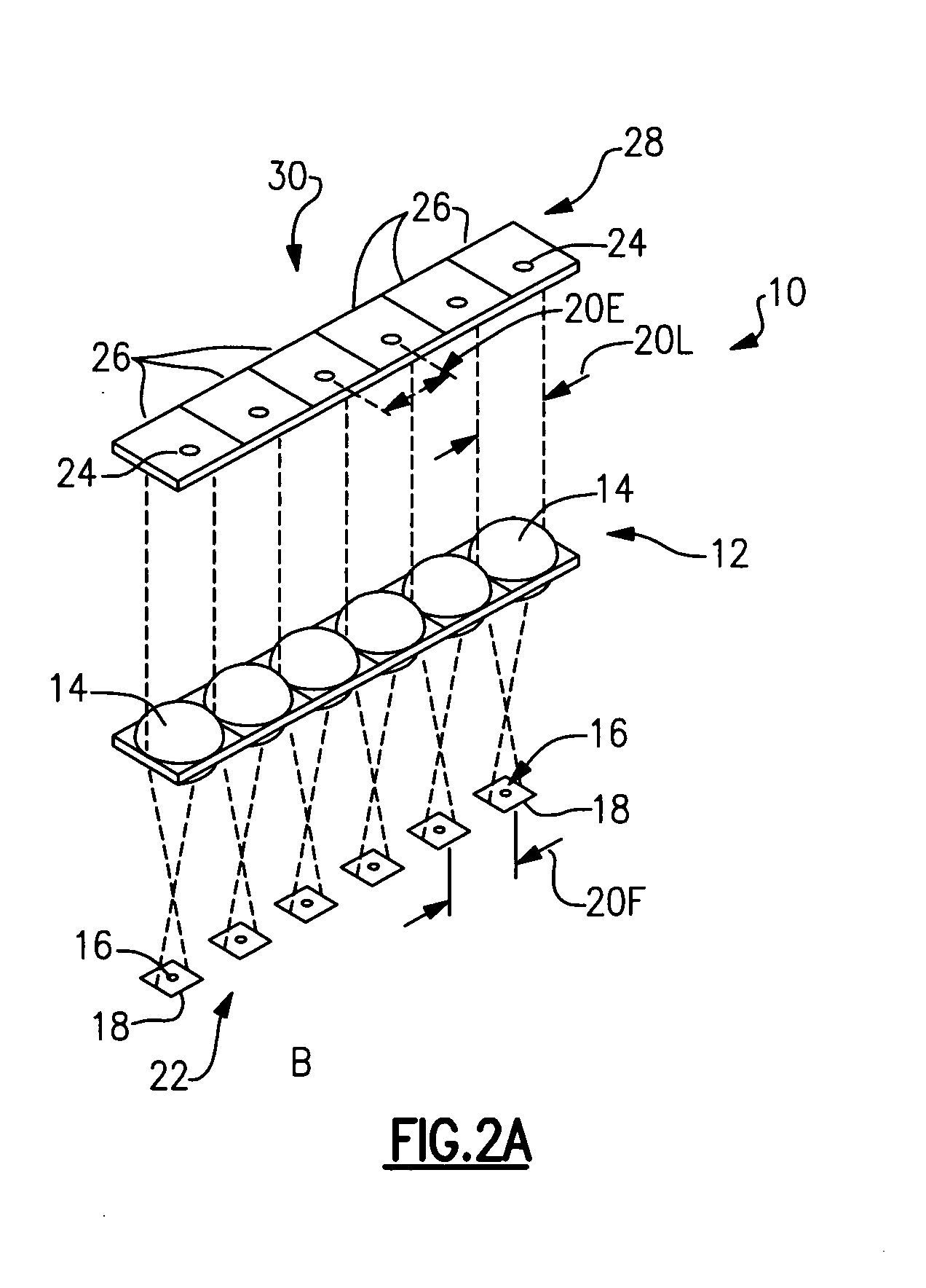
[0030]As will be described in the following, the present invention concerns a system and method providing an increased pixel resolution over the diameter of the microvias while, at the same time, increasing the inspection processing throughput. A system of the present is configurable, for example, as either a linear two dimensional (2D) imaging Charge Coupled Device (CCD) camera or as two dimensional (2D) CCD array camera to image microvias or blind hole vias in either a continuous scan process or in a “step and repeat” process. The system and method of the present invention may also be used to image and inspect conductor traces or through hole via interconnects within multi-layer printed circuit board assemblies (PCBs) as are commonly used within the high density printed circuit board industry.

[0031]The following descriptions will focus, however, on the inspection of microvias and the detection of defects, such as partially drilled microvias, as presenting the most difficult inspec...


PUM


Abstract

An imaging method and imaging system for inspecting features located at a known inter-feature pitch on portions of a target surface. The system includes a lens array having a plurality of lenses wherein the lenses of the lens array have an inter-lens pitch and an inter-field of view pitch corresponding to the inter-feature pitch, and an array of imaging elements having an inter-element pitch corresponding to the inter-feature pitch, whereby the imaging system images only field of view areas of the target surface containing features.

Description

FIELD OF THE INVENTION[0001]The present invention relates to a method and apparatus for the scanning and imaging of features of interest on printed circuit boards and, more particularly, to a method and apparatus for image inspection of vias of a printed circuit board using imaging lens arrays and time delay and integration processing.BACKGROUND OF THE INVENTION[0002]The manufacture of high density microelectronic packages and devices, such as integrated chip packages (ICPs) or printed circuit boards for cell phones, requires the fabrication of single or multilayer printed circuit boards (PCBs) having high density arrays of small holes referred to as microvias. Microvias are formed using sophisticated mechanical and laser drilling systems and, once formed are plated to provide electrical connections and leads to and between the layers, circuits and circuit elements of single and multi-layer PCBs.[0003]Over the last several years the number of microvias that can be and are formed int...

Claims


Application Information

Patent Timeline
Patent Type & Authority Applications(United States)
IPC IPC(8): G02B27/10
CPCG01N21/8806G01N21/95692G01N2021/646G01N2021/95653G02B3/0062G02B3/0006G02B3/0031G02B3/005G02B3/0056G01N2201/0638
Inventor LIZOTTE, TODD E.
Owner HITACHI SEIKO LTD
Why Eureka
Try Eureka