


Quick Research
Generate reliable direction feasibility study reports for your R&D in just a few steps.

Technical Q&A
Discover and master advanced knowledge NOW. Basics, ideas, possibilities, all at once.

Find Solutions
As an expert in R&D theories, this can generate solutions to your technical problems instantly.

Evaluate Feasibility
Analyze your overall solution with one click, know your potential R&D risks in advance.

Monitor Landscape
Get weekly tech updates, stay abreast of the latest tech innovations and key insights.
Magnetoresistance Element Magnetic Random Access Memory, Magnetic Head and Magnetic Storage Device
a technology of magnetic random access memory and magnetoresistance element, which is applied in the field of magnetoresistance element, magnetic random access memory, magnetic head and magnetic storage device, can solve the problems of deteriorating magnetoresistance characteristics, interdiffusion of elements of film stack, and reducing the mr ratio, so as to avoid diffusion, suppress diffusion, and low specific resistance
- Summary
- Abstract
- Description
- Claims
- Application Information
AI Technical Summary
Benefits of technology
Problems solved by technology
Method used
Image

Examples
first embodiment
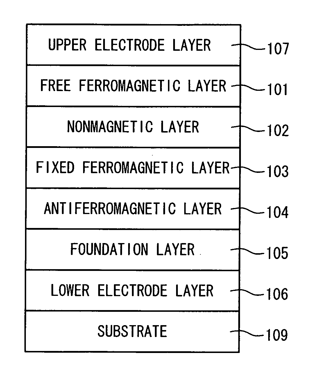
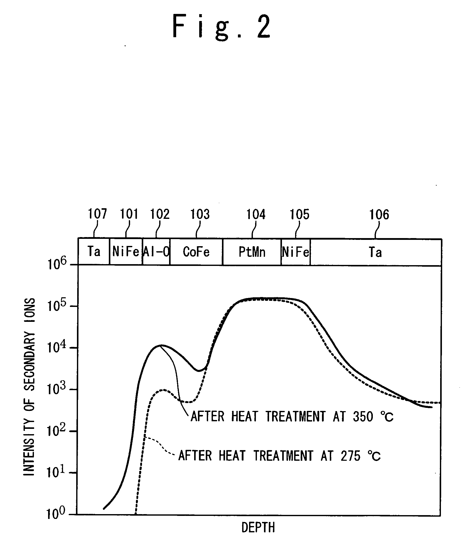
[0093]FIG. 23 is a chart showing embodiments of the present invention with the structure of FIG. 9. The lower electrode layer 6, the foundation layer 5, the antiferromagnetic layer 4, the fixed ferromagnetic layer 3, the nonmagnetic layer 2, the free ferromagnetic layer 1 and the upper electrode layer 7 are composed of materials described in the chart, respectively. Numbers described in the parentheses indicate film thicknesses (nm). The respective films are formed by a sputtering method. The ultimate pressure is 7×10⁻⁷ Pa, and the sputtering gas pressure (Ar) is 0.3 Pa. The sputtering electric power is set to 300 W. It should be noted that an Al—O film as the nonmagnetic layer 2 is subjected to oxidization with plasma generated by feeding high frequency electric power of 300 W to Ar gas atmosphere containing oxygen after film formation of metal aluminum. The sputtering gas and the gas used for the oxidization are not limited to Ar; Kr or Xe may be used instead. Thereafter, the magn...
second embodiment
[0095]FIG. 24 is a chart showing embodiments of the present invention with the structure of FIG. 9. The lower electrode layer 6, the foundation layer 5, the antiferromagnetic layer 4, the fixed ferromagnetic layer 3, the nonmagnetic layer 2, the free ferromagnetic layer 1 and the upper electrode layer 7 are composed of materials described in the chart, respectively. Numbers described in parentheses indicate film thicknesses (nm). The respective films are formed by a sputtering method. The ultimate pressures (Pa) and the sputtering gas (Ar) pressures (Pa) are described in the chart, respectively. Other conditions are as explained in FIG. 23.
[0096] As shown in FIG. 24, the small MR ratios of about 10% are obtained after heat treatment at 350° C. for 30 minutes conducted thereafter with respect to the comparative examples, while large MR ratios of about 40% or larger are obtained with respect to the structure (FIG. 9) according to the present invention. These values are large enough t...
third embodiment
[0097]FIG. 25 is a chart showing embodiments of the present invention with the structures of FIGS. 10 to 13. The lower electrode layer 6, the foundation layer 5, the antiferromagnetic layer 4, the fixed ferromagnetic layer 3, the nonmagnetic layer 2, the free ferromagnetic layer 1 and the upper electrode layer 7 are composed of materials described in the chart, respectively. Numbers described in the parentheses indicate film thicknesses (nm). The respective films are formed by a sputtering method. The ultimate pressure is 7×10⁻⁷ Pa, and the sputtering gas pressure (Ar) is 0.3 Pa. The sputtering electric power is set to 300 W. Other conditions are as explained in FIG. 23.
[0098] As shown in FIG. 25, small MR ratios of about 10% are obtained after heat treatment at 350° C. for 30 minutes conducted thereafter with respect to the comparative examples, while large MR ratios of about 40% or larger are obtained with respect to the structures (FIGS. 10 to 13) according to the present invent...
PUM
 Abstract
Description
Claims
Application Information
 - R&D Engineer
- R&D Manager
- IP Professional
- Industry Leading Data Capabilities
- Powerful AI technology
- Patent DNA Extraction
Browse by: Latest US Patents, China's latest patents, Technical Efficacy Thesaurus, Application Domain, Technology Topic, Popular Technical Reports.
© 2024 PatSnap. All rights reserved.Legal|Privacy policy|Modern Slavery Act Transparency Statement|Sitemap|About US| Contact US: help@patsnap.com