
Biological information detection sensor device

a biological information and sensor technology, applied in the field of biological information processing devices, can solve the problems of adverse effects on the skin of the human body, unsanitary contact of biological information detection sensors with the human body, etc., and achieve the effects of easy replacement, easy cleaning, and electric characteristic of transistors

Inactive Publication Date: 2008-03-27
SEMICON ENERGY LAB CO LTD
View PDF25 Cites 42 Cited by
  • Summary
  • Abstract
  • Description
  • Claims
  • Application Information

AI Technical Summary

Benefits of technology

[0006] It is an object of the present invention to provide a biological information detection sensor device which can be easily replaced.
[0014] Since the biological information detection sensor device of the present invention is directly in contact with the skin of the human body, an external side thereof might easily get dirty due to sweat or the like. In addition, a semiconductor layer of a transistor included in the biological information detection sensor device might be contaminated by an alkali metal element contained in sweat, and accordingly, an electric characteristic of the transistor might be deteriorated. However, according to the present invention, even if the biological information detection sensor gets dirty, it can be easily replaced with a new one, thereby being sanitary.
[0015] In addition, the biological information detection sensor system of the present invention can be manufactured at low costs; therefore, it is easy to replace it with a new one, and people can constantly put on a sanitary biological information detection sensor.

Problems solved by technology

It is unsanitary that the biological information detection sensor is constantly in contact with the human body, and it might have an adverse effect on the skin of the human body.

Method used


Image

  • Biological information detection sensor device
  • Biological information detection sensor device
  • Biological information detection sensor device

Examples


embodiment 1

[0053] In this embodiment, an example in which a biological information detection sensor of the present invention is applied to infants including newborn babies with reference to FIGS. 4A to 4D.

[0054] Newborn babies 201 (201a, 201b, 201c, and so on) lie on beds 204 placed in a nursery room 205 of a hospital (see FIG. 4A). A biological information detection sensor system 211 is attached to a wrist 202 of the newborn baby 201 (see FIG. 4B).

[0055] The biological information detection sensor system 211 has the structure described in Embodiment Mode. That is, the biological information detection sensor 212 is attached to the wrist 202 by an adhesive tape 214. The biological information detection sensor 212 is provided with an antenna 213 for sending and receiving. The antenna 213 is pulled from an adhesive surface to a surface through a groove provided in the adhesive tape 214, and is fixed to the surface of the adhesive tape 214 by a fixation mechanism provided on the surface of the a...

embodiment 2

[0063] In this embodiment, an example in which an ID chip (also referred to as an IC tag or an IC chip) is manufactured by the present invention will be described with reference to FIGS. 5A and 5B, FIGS. 6A and 6B, FIGS. 7A and 7B, and FIGS. 8A and 8B.

[0064] In this embodiment, a TFT that is insulated and isolated is exemplified as a semiconductor element; however, a semiconductor element used for an integrated circuit is not limited thereto, and all circuit elements can be used. For example, a memory element, a diode, a photoelectric conversion element, a resistance element, a coil, a capacitor element, an inductor, and the like are typically given, besides a TFT.

[0065] First, a separation layer 402 is formed over a substrate (a first substrate) 401 having heat resistance by a sputtering method. For example, as the first substrate 401, a glass substrate such as barium borosilicate glass or aluminoborosilicate glass, a quartz substrate, a ceramic substrate, or the like can be used...

embodiment 3

[0146] In this embodiment, an example of manufacturing an ID chip (also referred to as an IC chip or an IC tag) incorporated in a biological information detection sensor of the present invention which differs from that in Embodiment 2 will be explained with reference to FIGS. 9A and 9B, FIGS. 10A and 10B, FIGS. 11A and 11B, and FIGS. 12A and 12B.

[0147] In this embodiment, a TFT that is insulated and isolated is exemplified as a semiconductor element; however, a semiconductor element used for an integrated circuit is not limited thereto, and all circuit elements can be used. For example, a memory element, a diode, a photoelectric conversion element, a resistance element, a coil, a capacitor element, an inductor, and the like are typically given, besides a TFT.

[0148] First, a separation layer 602 is formed over a substrate (a first substrate) 601 having heat resistance by a sputtering method. For example, as the first substrate 601, a glass substrate such as barium borosilicate glas...


PUM


Abstract

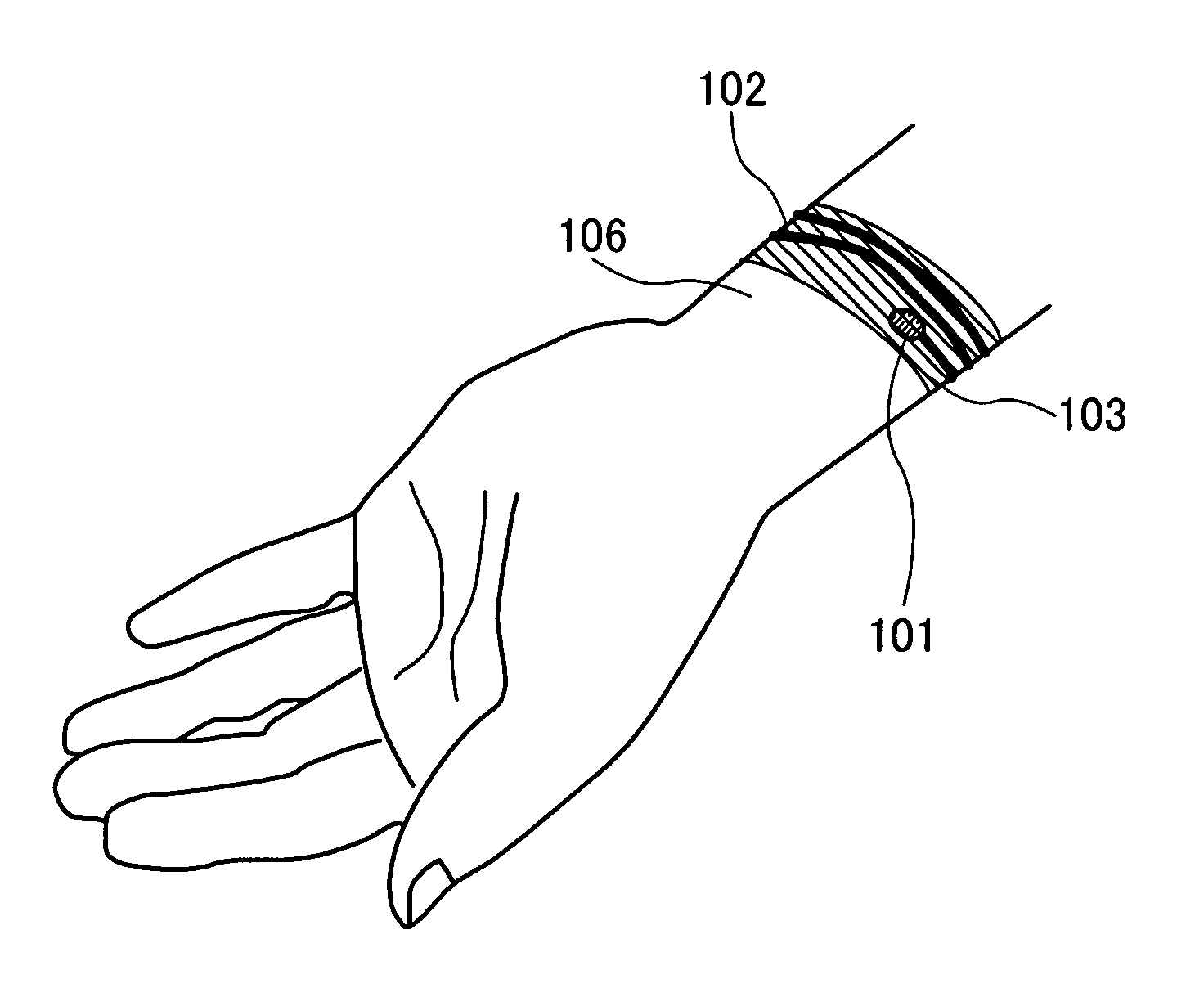
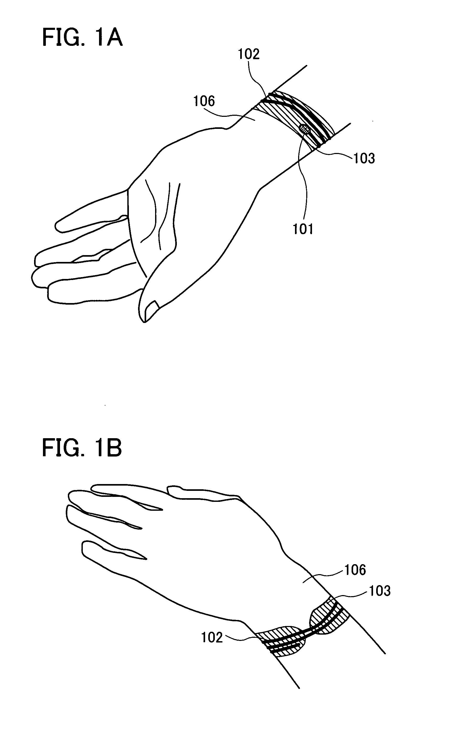
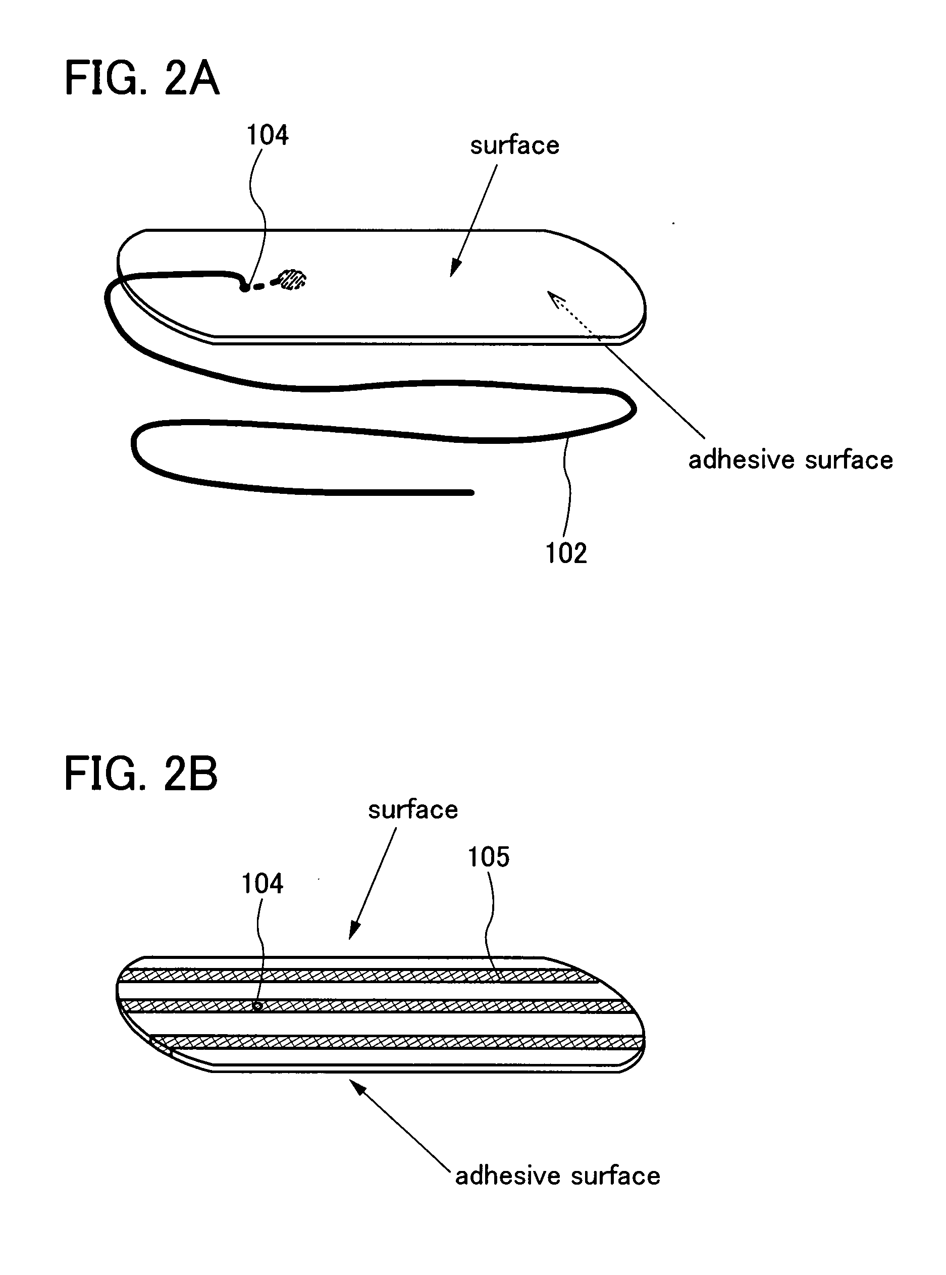
It is an object of the present invention to provide a biological information detection sensor system which can be easily replaced. The present invention relates to a biological information detection sensor system having an adhesive tape including an adhesive surface which is provided with an adhesive material and a surface which is not provided with the adhesive material; a biological information detection sensor having an ID tag in which personal information is stored and a sensor, which is attached to an adhesive surface side of the adhesive tape; and an antenna which is connected to the biological information detection sensor and is pulled from the adhesive surface of the adhesive tape to the surface thereof through a groove provided in the adhesive tape. Accordingly, even if the biological information detection sensor gets dirty, it can be replaced to a new one soon, thereby being sanitary.

Description

BACKGROUND OF THE INVENTION [0001] 1. Field of the Invention [0002] The present invention relates to a biological information processing device which can detect biological information (an electric signal) of the human body by a biological information detection sensor attached to the human body, send the detected biological information, and communicate the detected or sent biological information with an external device. [0003] 2. Description of the Related Art [0004] In recent years, in order to respond the demand of medical check-up or the like, a biological information detection sensor which is attached to a site to be detected of a user and detects biological information has been developed, and downsizing of the biological information detection sensor is developing in combination with downsizing of an electronic device (see Patent Document 1: Japanese Published Patent Application No. 2003-275183). SUMMARY OF THE INVENTION [0005] It is unsanitary that the biological information det...

Claims


Application Information

Patent Timeline
Patent Type & Authority Applications(United States)
IPC IPC(8): A61B5/00A61B5/04
CPCA61B5/0002A61B5/0008A61B2562/08A61B2560/0219A61B5/6833
Inventor YAMAZAKI, SHUNPEIARAI, YASUYUKIKOMORI, MIHO
Owner SEMICON ENERGY LAB CO LTD
Learn More