Beam line architecture for ion implanter

a technology of ion implanter and beam, which is applied in the field of ion implanter control, can solve the problems of small error margins, achieve uniform and precise implant properties across the wafer, facilitate filtration of neutral contaminants, and maintain relatively high beam energy

Active Publication Date: 2008-04-03
AXCELIS TECHNOLOGIES
View PDF42 Cites 26 Cited by
  • Summary
  • Abstract
  • Description
  • Claims
  • Application Information

AI Technical Summary

Benefits of technology

[0007]A parallelizing component comprising two dipole magnets bends a scanned ion beam traversing therethrough such that the ion beam trajectory has a substantially “s” shape. This s-bend serves to facilitate uniform and precise implant properties across the wafer, such as implant angle, for example, while facilitating filtration of neutral contaminants of the beam. Additionally, a deceleration stage is included toward the end of the implantation system so that the energy of the beam can be kept relatively high throughout the beamline to mitigate beam blowup. This deceleration stage also facilitates filtering neutral and energetic contaminants out of the beam.

Problems solved by technology

Additionally, there may be smaller margins for error with regard to the orientation (e.g., angle) of the ion beam relative to the mechanical surface and / or crystalline lattice structure of the workpiece.

Method used


Image

  • Beam line architecture for ion implanter
  • Beam line architecture for ion implanter
  • Beam line architecture for ion implanter

Examples


Embodiment Construction

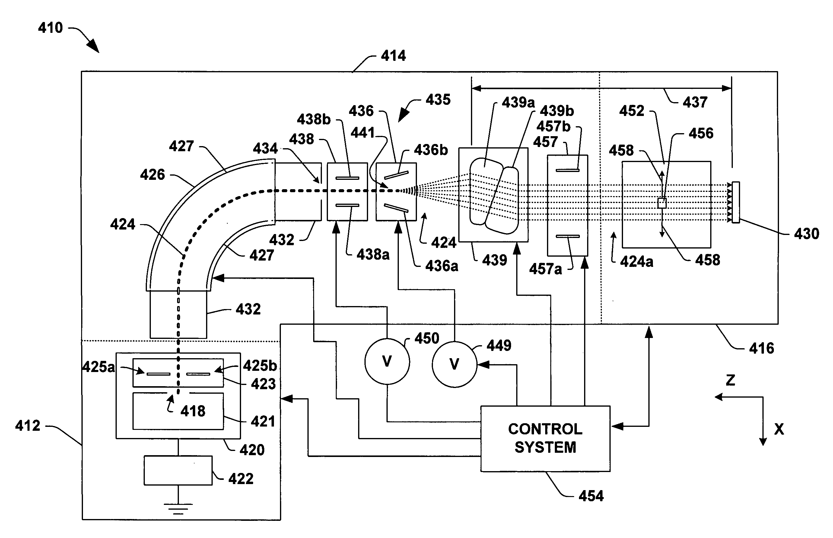
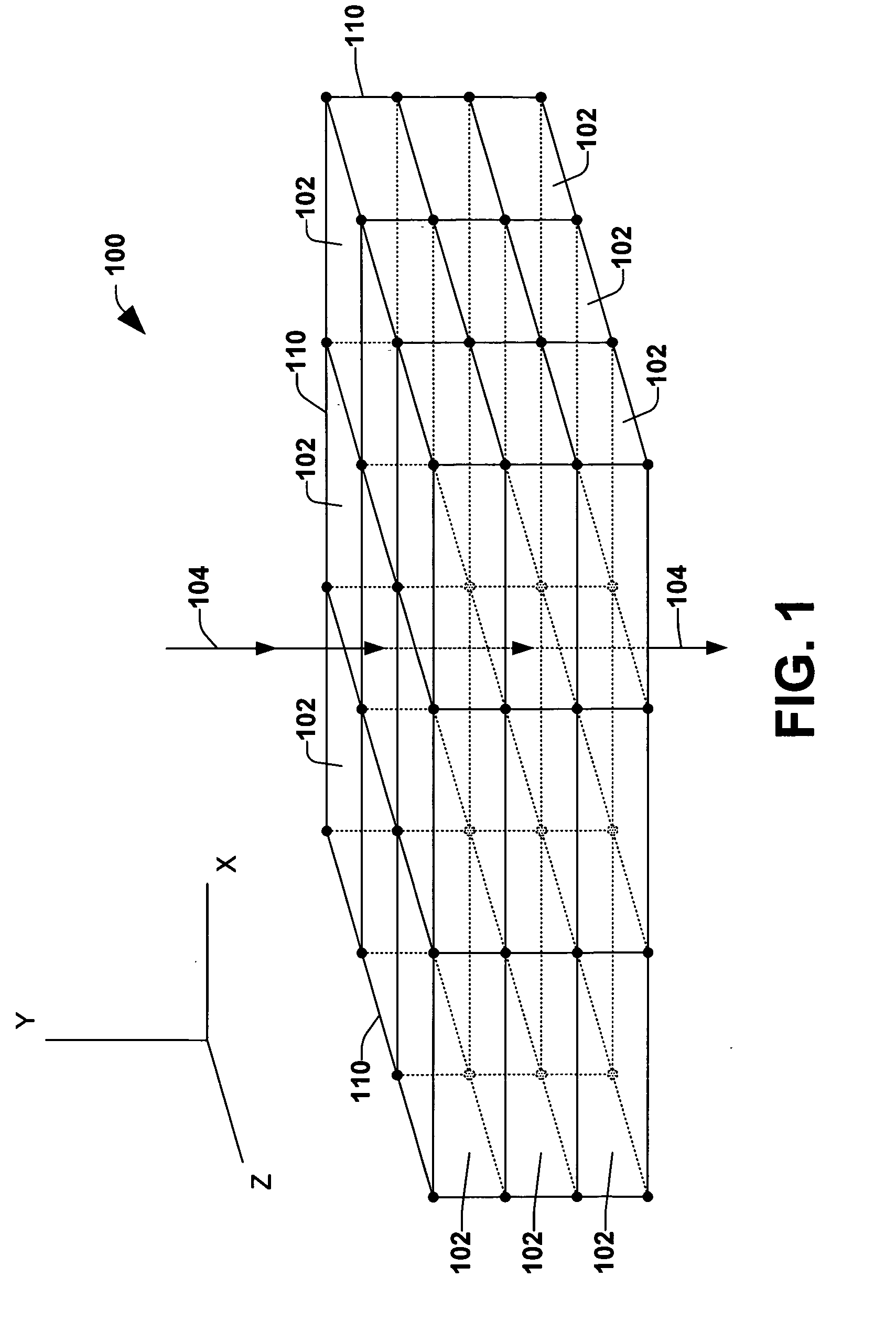
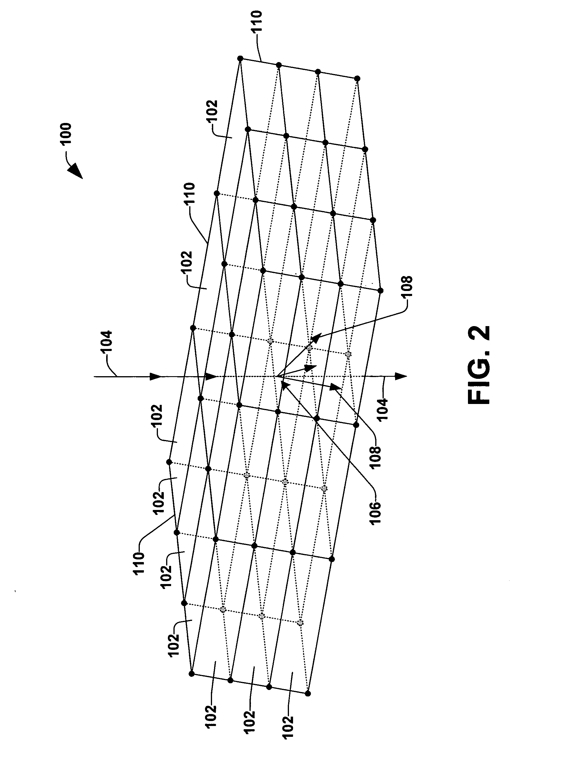
[0017]One or more aspects of the present invention are described with reference to the drawings, wherein like reference numerals are generally utilized to refer to like elements throughout, and wherein the various structures are not necessarily drawn to scale. In the following description, for purposes of explanation, numerous specific details are set forth in order to provide a thorough understanding of one or more aspects of the present invention. It may be evident, however, to one skilled in the art that one or more aspects of the present invention may be practiced with a lesser degree of these specific details. In other instances, well-known structures and devices are shown in block diagram form in order to facilitate describing one or more aspects of the present invention.

[0018]As alluded to above, in semiconductor fabrication processing, semiconductor wafers or workpieces are implanted with charged particles or ions. The implanted materials are referred to as dopants because t...


PUM


Abstract

A parallelizing component of an ion implantation system comprises two angled dipole magnets that mirror one another and serve to bend an ion beam traversing therethrough to have a substantially “s” shape. This s bend serves to filter out contaminants of the beam, while the dipoles also parallelize the beam to facilitate uniform implant properties across the wafer, such as implant angle, for example. Additionally, a deceleration stage is included toward the end of the implantation system so that the energy of the beam can be kept relatively high throughout the beamline to mitigate beam blowup.

Description

FIELD OF THE INVENTION[0001]The present invention relates generally to ion implantation systems, and more particularly to controlling an ion beam in an ion implanter.BACKGROUND OF THE INVENTION[0002]Ion implantation systems are mechanisms utilized to dope semiconductor substrates with impurities in integrated circuit manufacturing. In such systems, a dopant material is ionized and an ion beam is generated there-from. The ion beam is directed at the surface of a semiconductor wafer or workpiece to implant ions into the wafer. The ions of the beam penetrate the surface of the wafer and form regions of desired conductivity therein, such as in transistor fabrication, for example. A typical ion implanter includes an ion source for generating the ion beam, a beamline assembly including a mass analysis apparatus for directing and / or filtering (e.g., mass resolving) ions within the beam, and a target chamber containing one or more wafers or workpieces to be treated.[0003]Batch type of impla...

Claims


Application Information

Patent Timeline
Patent Type & Authority Applications(United States)
IPC IPC(8): H01J37/317
CPCH01J37/04H01J37/1471H01J37/304H01J37/3171H01J2237/0475H01J2237/31703H01J2237/1501H01J2237/152H01J2237/24507H01J2237/24528H01J2237/3045H01J2237/055H01J37/30H01L21/265
Inventor VANDERBERG, BO H.SPLINTER, PATRICK
Owner AXCELIS TECHNOLOGIES
Why Eureka
Try Eureka