Through-silicon via and method for forming the same

a technology of throughsilicon via and stacked chips, which is applied in the direction of semiconductor devices, semiconductor/solid-state device details, electrical devices, etc., can solve the problems of difficult to obtain uniformity and low roughness, difficult to secure a thickness for obtaining satisfactory insulation characteristics, and high cost of oxide layer formed through high-temperature dry oxidization and wet oxidization processes or nitride layers. achieve the effect of reducing the cost of forming

Inactive Publication Date: 2008-04-03
SK HYNIX INC
View PDF5 Cites 140 Cited by
  • Summary
  • Abstract
  • Description
  • Claims
  • Application Information

AI Technical Summary

Benefits of technology

[0012]The present invention is directed to a TSV which can reduce the cost of forming an insulation layer in the manufacture of a stack package using the TSV, and a method for forming the same.
[0013]Also, the present invention is directed to a TSV which can secure an insulation characteristic of an insulation layer in the manufacture of a stack package using a TSV, and a method for forming the same.
[0014]Further, the present invention is directed to a TSV which can secure uniformity and low roughness of an insulation layer in the manufacture of a stack package using a TSV, and a method for forming the same.
[0015]Still, the present invention is directed to a TSV which can secure an excellent mechanical characteristic of an insulation layer in the manufacture of a stack package using a TSV, and a method for forming the same.
[0016]Additionally, the present invention is directed to a TSV which can prevent a defect from being caused in a semiconductor device due to the flaw of an insulation layer in the manufacture of a stack package using a TSV, and a method for forming the same.

Problems solved by technology

The oxide layer formed through the high-temperature dry oxidization and wet oxidization processes or the nitride layer is relatively expensive.
Also, while a proper thickness is required to secure an insulation characteristic, when considering the size of the vertical hole, it is difficult to secure a thickness for obtaining a satisfactory insulation characteristic.
In addition, since the layer must be formed in the vertical hole, it is difficult to obtain uniformity and low roughness.
Moreover, the oxide layer formed through the high temperature dry oxidization and wet oxidization processes or the nitride layer is difficult to compensate for a difference in mechanical characteristic between the electrolytic substance in the vertical hole and silicon.
Different thermal expansion coefficients between silicon and a metal or metallic substance can causes stresses in a semiconductor chip as its temperature rises and falls during operation, which is a phenomena that can significantly deteriorate the integrity and hence the reliability of silicon / metal junctions in a chip during the operation of the semiconductor chip.
As a consequence, if the insulation layer cannot relieve the fatigue caused due to the difference in thermal expansion coefficient, displacements of respective materials vary when operation temperature is changed, and a fatigue is caused, by which fracture of a package may result.
In this regard, the oxide layer or the nitride layer cannot appropriately relieve the fatigue caused due to the difference in thermal expansion coefficient between materials, as a result of which the fracture of the package may not be avoided.
Furthermore, in the oxide layer formed through the high temperature dry oxidization and wet oxidization processes or the nitride layer, when a defect is produced therein, a crack starting from the defect can be easily propagated into silicon, thereby causing a defect in a chip.

Method used


Image

  • Through-silicon via and method for forming the same
  • Through-silicon via and method for forming the same
  • Through-silicon via and method for forming the same

Examples


Embodiment Construction

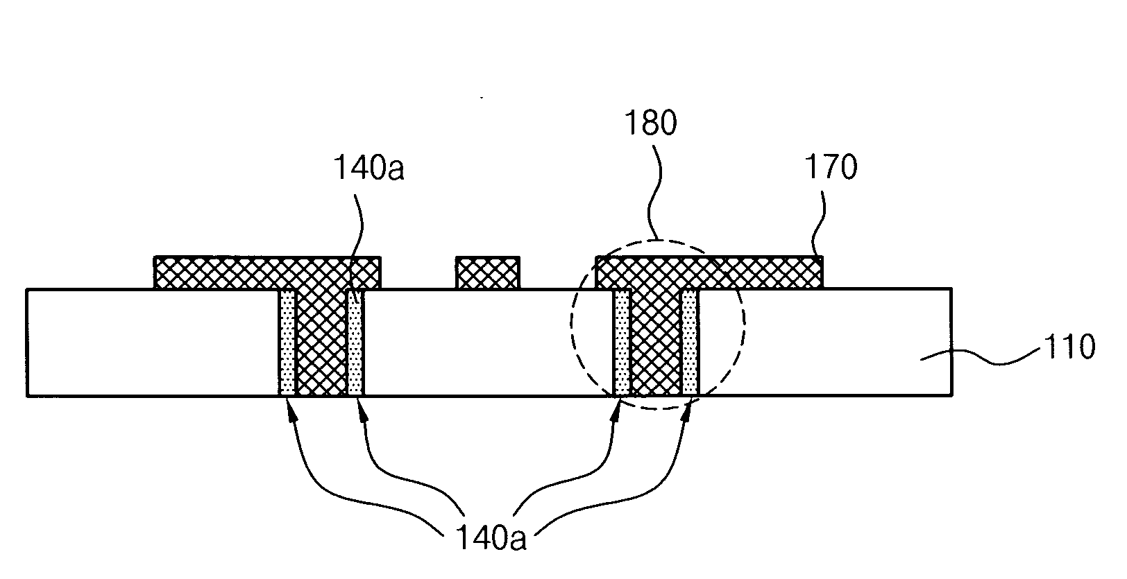
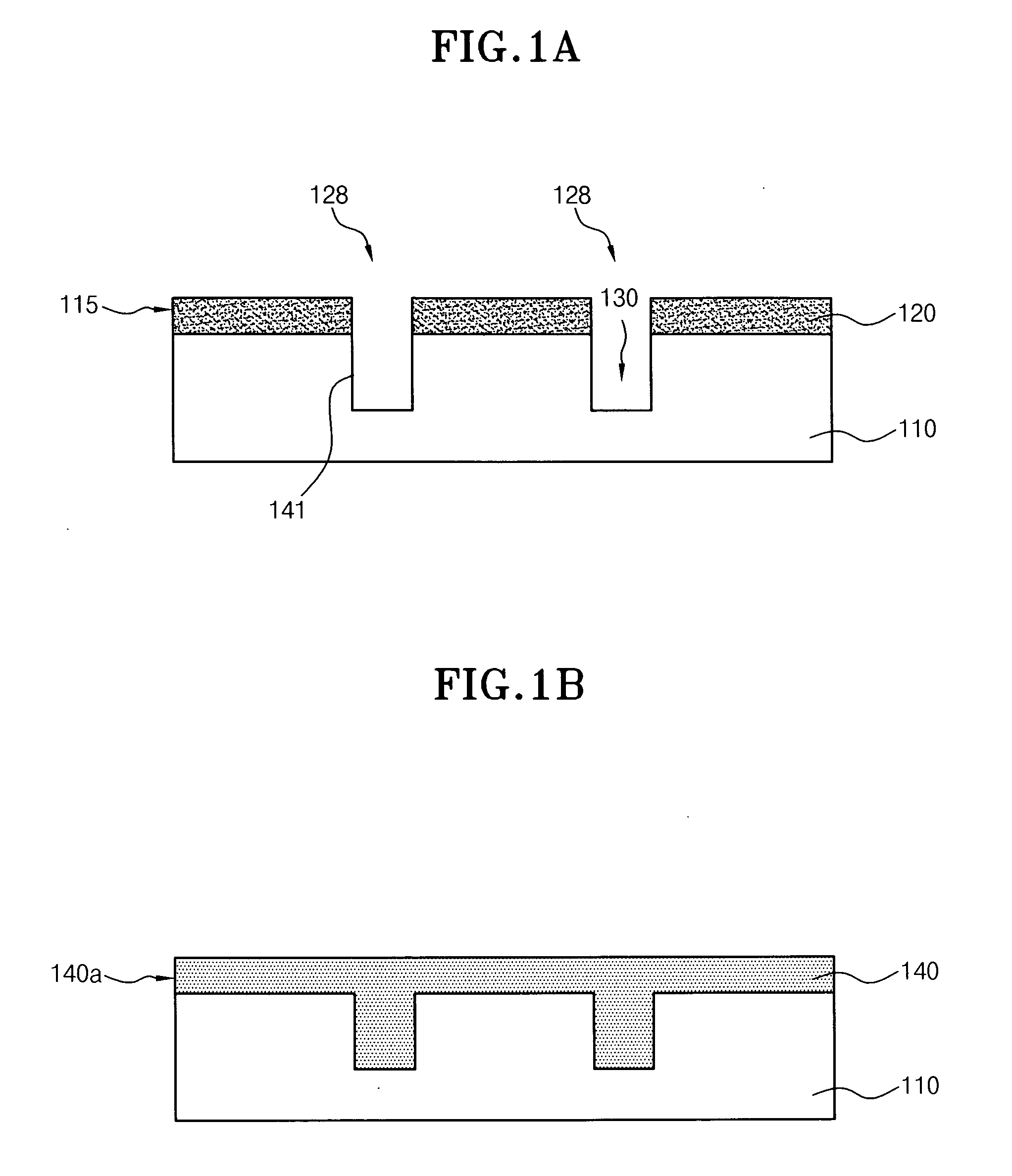
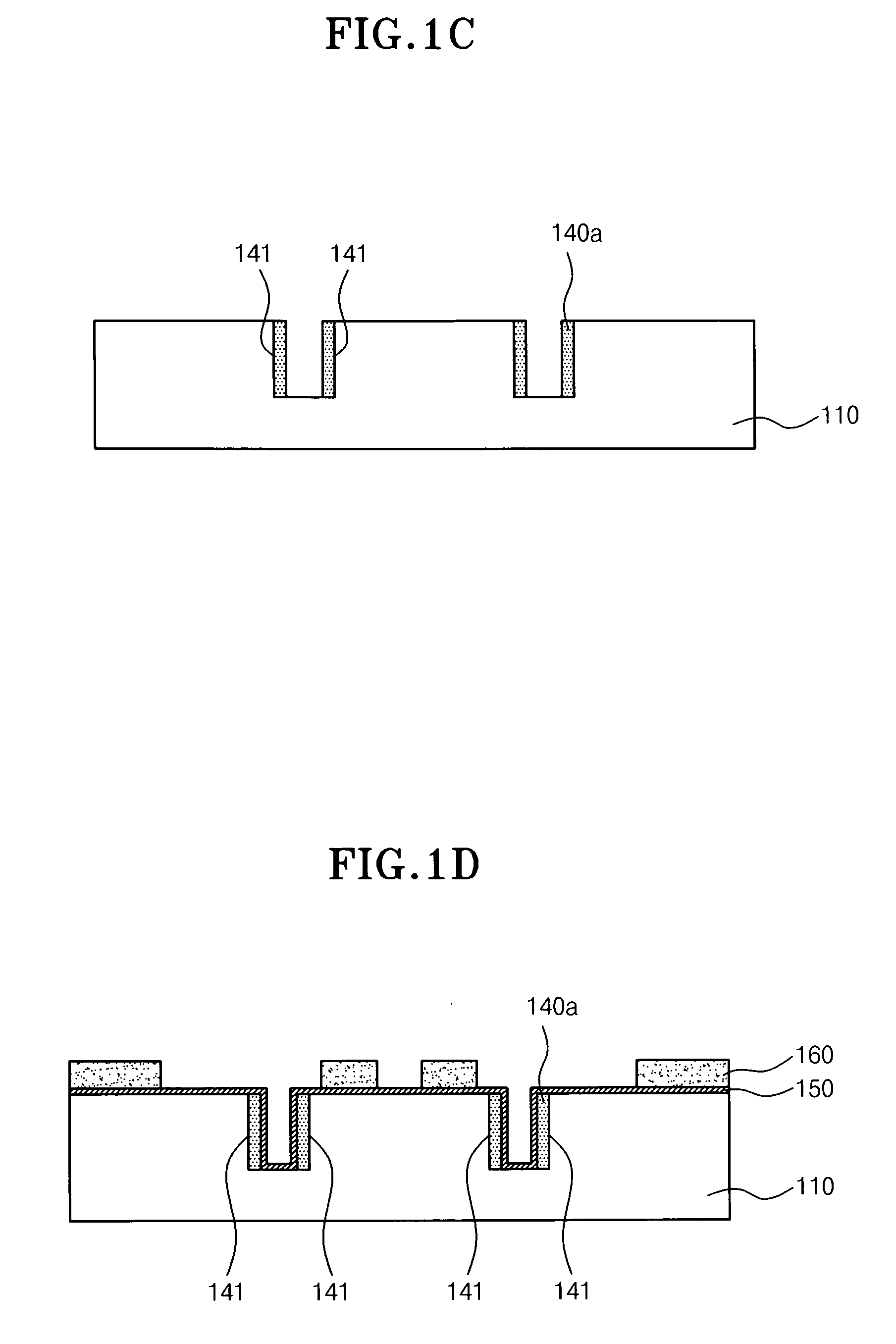
[0023]In the present invention, a relatively flexible polymer which adheres to both the surface of a silicon through-hole but also to a metal or metallic substance that is deposited over the polymer coating a silicon surface, provides a flexible, mechanical interface between silicon and a metal or metallic filler, which can accommodate variations in thermal expansion coefficients between silicon and the metal or metallic substance to provides improved mechanical compliance. The polymer also forms an insulation layer between silicon and an electrolytic or metallic substance. Such a polymer is referred to herein as a polymer that has “mechanical compliance” or which is “mechanically compliant.” That is to say, in the present invention, after filling a vertical hole defined for forming a vertical connection with liquid polymer, through patterning the polymer to a desired shape using a photolithography process, an insulation layer is formed.

[0024]In this case, since the liquid polymer i...


PUM


Abstract

A method for forming a through-silicon via includes the steps of defining a groove in each chip of a wafer which has a plurality of semiconductor chips; applying liquid polymer on the wafer to fill the groove; forming an insulation layer on a sidewall of the groove through patterning the polymer; forming a metal layer to fill the groove which is formed with the insulation layer on the sidewall thereof; and back-grinding a backside of the wafer to expose the metal layer filled in the groove.

Description

CROSS-REFERENCE TO RELATED APPLICATIONS[0001]The present application claims priority to Korean patent application number 10-2006-0096718 filed on Sep. 30, 2006, which is incorporated herein by reference in its entirety.BACKGROUND OF THE INVENTION[0002]The present invention relates to a stack package, and more particularly to a through-silicon via for connection of stacked chips and a method for forming the same.[0003]Packaging technology for an integrated circuit has continuously been developed to meet the demand toward miniaturization and mounting reliability. Recently, as the miniaturization and high functionality of electric / electronic products are required, various techniques have been disclosed in the art.[0004]The term “stack” in the semiconductor industry means a vertical stand or pile of at least two chips or packages, one atop the other. By using a stack, in the case of a memory device for example, it is possible to produce a product having a memory capacity which is two ti...

Claims


Application Information

Patent Timeline
Patent Type & Authority Applications(United States)
IPC IPC(8): H01L29/40H01L21/76
CPCH01L2224/02372H01L21/76898H01L21/28
Inventor HAN, KWON WHAN
Owner SK HYNIX INC
Why Eureka
Try Eureka