Plane structure of light-emitting diode lighting apparatus
a technology of light-emitting diodes and lighting apparatuses, which is applied in the direction of lighting and heating apparatus, lighting support devices, dielectric characteristics, etc., can solve the problems of limiting the size, dimensions, shape and viewing effect of an applied product, and achieve the effect of improving the prettification and diversion effect and enhancing the stereo design
- Summary
- Abstract
- Description
- Claims
- Application Information
AI Technical Summary
Benefits of technology
Problems solved by technology
Method used
Image
Examples
first embodiment
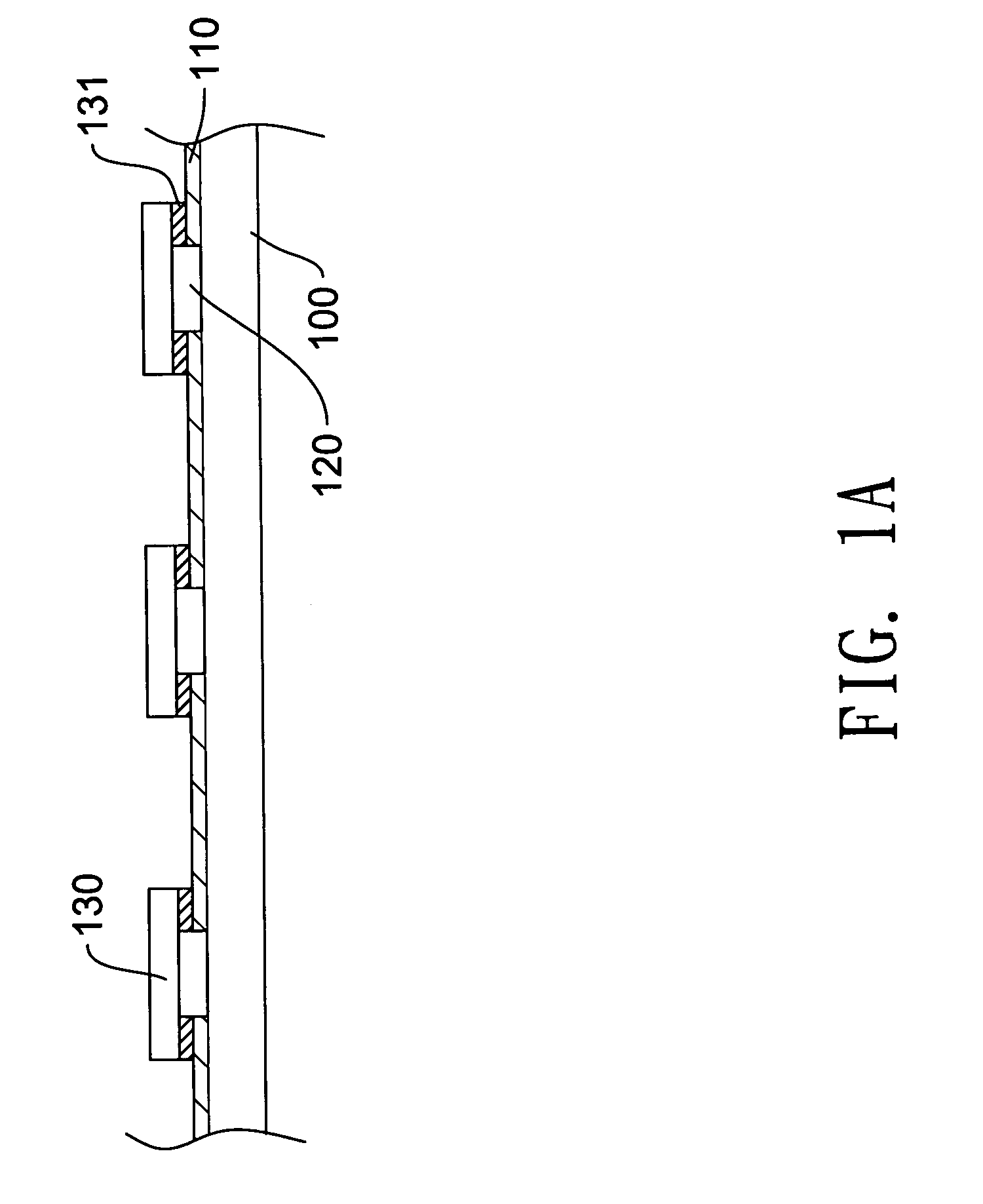
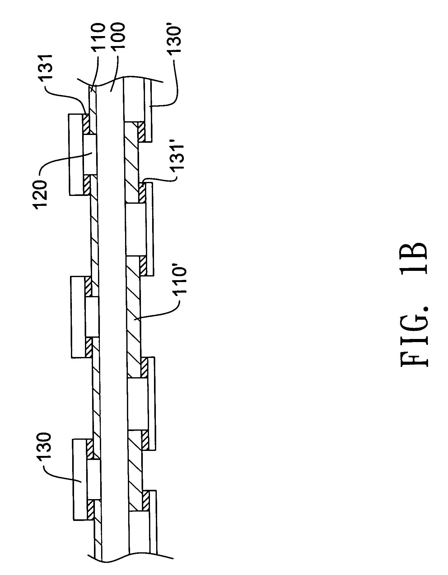
[0021]FIG. 1A is a cross-sectional diagram of a plane structure of an LED lighting apparatus in accordance with the present invention. An LED lighting apparatus includes a first transparent pattern and a second transparent pattern 120 on a transparent flexible tape 100. One or more first LEDs 130 are attached to the first transparent pattern with adhesive structures 131. In one embodiment, the transparent flexible tape 100 is made of insulating and flexible material, such as poly (ethylene terephthalate) (PET), poly carbonate (PC), oriented polypropylene (OPP), poly vinylchlorid (PVC), acrylic or other polymer material, but not limited to. Next, the first transparent pattern, such as a first transparent conductive line 110, but not limited to, is made of such as ITO (Indium Tin Oxide), IZO (Indium Zinc Oxide), or acrylic transparent conductive gel, which is formed on the transparent flexible tape 100 by silk screening or printing. It is appreciated that the first transparent conduct...
third embodiment
[0024]FIG. 2A is a cross-sectional diagram illustrating the plane structure of the LED lighting apparatus in accordance with the present invention. A first transparent pattern is disposed on a transparent flexible tape 400, and, in this embodiment, the first transparent pattern is a transparent conductive film 420, which is divided into a first zone 460 and a second zone 470 by a second transparent pattern 410. In the embodiment, the transparent conductive film 420, not limited to, is made of transparent conductive material such as ITO or IZO, which is formed on the transparent flexible tape 400 by sputtering, evaporate plating, printing or attaching. It is understood that the transparent conductive film 420 may be made with a conductive material implanted a dye or dyes for visual arts. Next, the second transparent pattern 410 will be formed on the transparent conductive film 420 as an insulating pattern by a suitable method, such as laser, chemically etching, printing or cutting, t...
PUM
 Abstract
Description
Claims
Application Information


