Storage Element

a technology of storage elements and elements, applied in the field of storage elements, can solve the problems of difficult vaporization of novel materials, inability to use ordinary film deposition methods, etc., and achieve the effects of improving the density of memory cells, high yield, and convenient manufacturing

Inactive Publication Date: 2008-04-10
SONY CORP
View PDF3 Cites 74 Cited by
  • Summary
  • Abstract
  • Description
  • Claims
  • Application Information

AI Technical Summary

Benefits of technology

[0043]Then, when the exposed surface is the surface of the semiconductor such as a silicon substrate, the surface of the substrate is polished with high precision and the exposed surface height has sufficient uniformity. For- this reason, patterning processing of the gate of a MOS transistor, for example, can be carried out with very high resolution at high precision.
[0060]Accordingly, it becomes possible to use materials of which characteristics such as resistance changing ratio are excellent and inexpensive materials for the resistance changing element. As a consequence, it becomes possible to easily discriminate information recorded on the memory cells of the storage element and to make the storage element inexpensive or to decrease a manufacturing cost.

Problems solved by technology

Thus, it is not possible to use ordinary film deposition methods (vapor deposition, sputtering, CVD method, etc.).
Then, when it is intended to process such novel material by the RIE method, it is difficult to vaporize such novel material depending on constitutive elements or even when such novel material can be vaporized, it is necessary to select reaction gas and to examine optimization of etching conditions and the like.

Method used


Image

  • Storage Element
  • Storage Element
  • Storage Element

Examples


Embodiment Construction

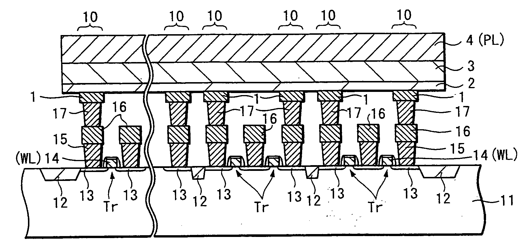
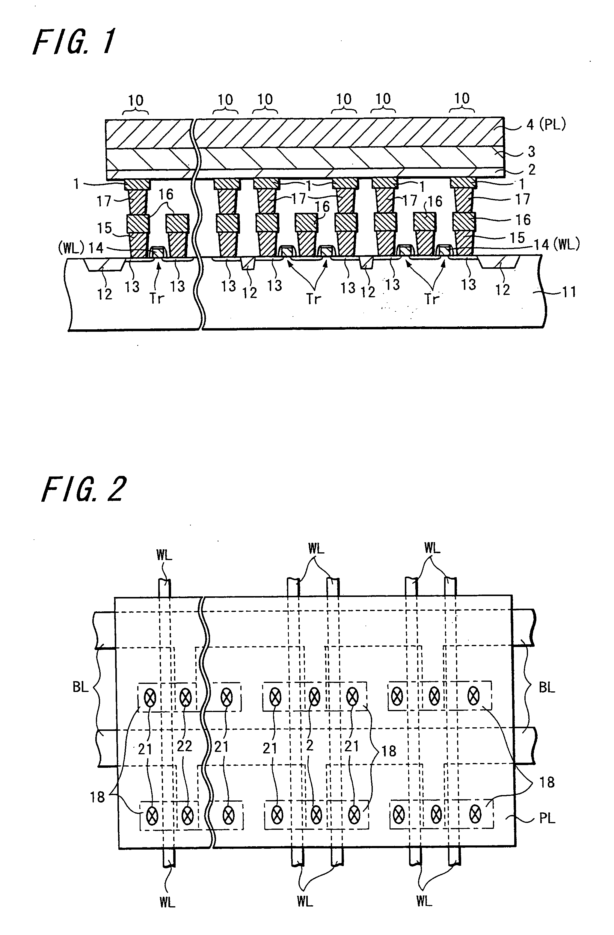
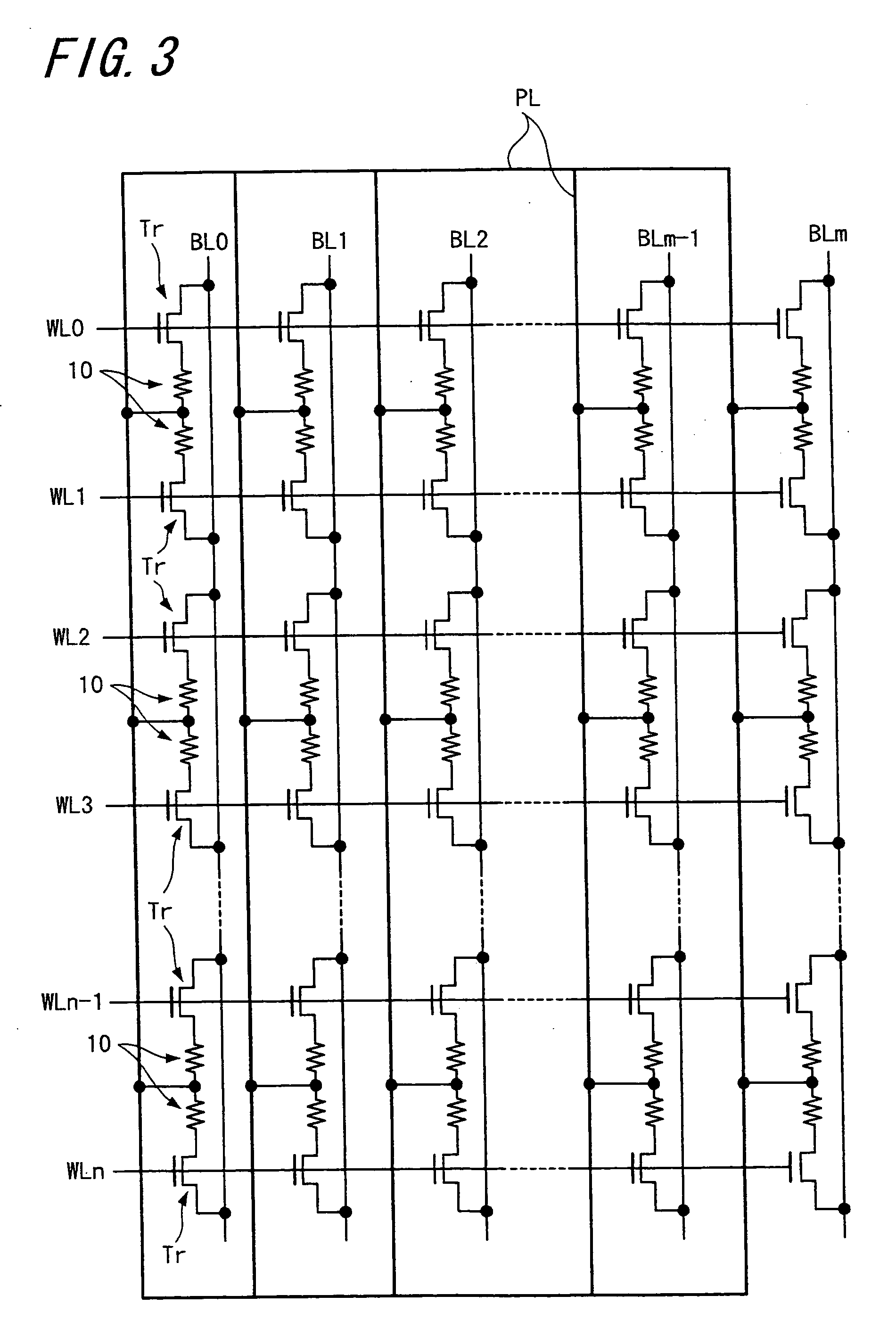
[0069]FIG. 1 is a schematic arrangement diagram (cross-sectional view) of a storage element according to an embodiment of the present invention.

[0070]This memory cell is composed of an array of a large number of resistance changing elements 10 which configure memory cells.

[0071]The resistance changing element 10 includes a high resistance film 2 and an ion source layer 3 sandwiched between a lower electrode 1 and an upper electrode 4. These high resistance layer 2 and ion source layer 3 constitute a recording layer by which information can be recorded on the resistance changing element 10 of each memory cell as will be described later on.

[0072]The ion source layer 3 contains more than one kind of elements (metal elements) selected from Ag, Cu, Zn and more than one kind of elements (chalcogenide elements) selected from S, Se, Te.

[0073]Then, when the metal element is ionized as will be described later on, a resistance value of the resistance changing element 10 is changed. That is, th...


PUM


Abstract

It is intended to provide a storage element having an arrangement which becomes able to be manufactured easily with high density.A storage element includes resistance changing elements 10 having recording layers 2, 3 provided between two electrodes 1, 4 and in which resistance values of the recording layers 2, 3 are reversibly changed with application of electric potential with different polarities to these two electrodes 1, 4, at least part of the layers 2, 3 constructing the recording layers of the resistance changing elements 10 being formed commonly by the same layer in a plurality of adjacent memory cells.

Description

FIELD OF THE INVENTION[0001]The present invention relates to a storage element in which memory cells are constructed by using resistance changing elements in which a resistance value of a recording film is reversibly changed with application of electric potential with different polarities to two electrodes.BACKGROUND ART[0002]In formation equipment such as computers, a high-density DRAM which can operate at a high speed is widely used as a random-access memory.[0003]However, the DRAM is complex in manufacturing process as compared with a general logic circuit LSI used in electronic equipment and signal processing and hence its manufacturing cost is high.[0004]Also, the DRAM is a volatile memory of which information is lost when the supply of power is stopped. Hence, refresh operation should be carried out frequently, that is, written information (data) should be read out, amplified again and information should be written again.[0005]For this reason, an FeRAM (ferroelectric substance...

Claims


Application Information

Patent Timeline
Patent Type & Authority Applications(United States)
IPC IPC(8): H01L45/00
CPCG11C13/0011H01L45/1675G11C2013/009G11C2213/56G11C2213/79H01L27/2436H01L27/2472H01L45/085H01L45/1233H01L45/1266H01L45/141H01L45/145H01L45/146H01L45/148H01L45/149G11C13/0069H10B63/82H10B63/30H10N70/245H10N70/8416H10N70/882H10N70/884H10N70/883H10N70/8845H10N70/8833H10N70/826H10N70/063H01L27/10
Inventor ARATANI, KATSUHISATSUSHIMA, TOMOHITONARISAWA, HIROAKIOTSUKA, WATARUHACHINO, HIDENARI
Owner SONY CORP
Why Eureka
Try Eureka