Display

a technology of display and display panel, applied in the field of display panel, can solve the problems of colour shift during extended operation, high cost of method, and high cost of required electronics circuitry, and achieve the effects of high brightness, high brightness, and no significant loss of efficiency

Inactive Publication Date: 2008-04-10
SHARP KK
View PDF13 Cites 92 Cited by
  • Summary
  • Abstract
  • Description
  • Claims
  • Application Information

AI Technical Summary

Benefits of technology

[0027]Use of a nanophosphor material as a re-emission source provides two advantages. Firstly, the emission spectrum of a nanophosphor material is narrow, typically with a full width at half maximum intensity (FWHM) of 80 nm or less. Secondly, the peak wavelength (and also the line-width) of the emission spectrum of a nanophosphor material can be chosen to be any desired value, by use of a suitable nanophosphor material (for example by controlling the size of the quantum dots, or the size distribution of the quantum dots, in the nanophosphor material). Accordingly, by making the emission spectrum of a nanophosphor material of the backlight such that the peak in the emission spectrum is centred, or substantially centred, within the transmission window of a respective colour filter (preferably a narrow passband colour filter), in the image display panel, it is possible to obtain a display that has a high NTSC ratio and a high brightness. FIGS. 2(c), 2(d) and 2(e) indicate that an NTSC ratio of over 110% may be obtained, without significant loss of efficiency.
[0028]To obtain a RGB display, the light source may be provided with red, green and blue nanophosphors that are illuminated by the primary light source, and the image display panel may have narrow passband red filters, narrow passband green filters, and narrow passband blue filters. Such a display is illustrated in FIG. 2(d), in which the left hand view shows the emission spectrum of the nanophosphors, and the central view shows the transmissivity of the colour filters of the liquid crystal panel. It can be seen that the emission spectrum is composed substantially of narrow red, green and blue emission peaks, and that the emission peaks in the spectrum of the nanophosphors in the left hand view of FIG. 2(d) are much narrower than the emission peaks in the spectrum of the conventional phosphors shown in the left hand view of FIG. 2(a); also, the intensity of emission in the green part of the spectrum is much higher for the nanophosphors. It can also be seen that each emission peak in the spectrum of the nanophosphors in the left hand view of FIG. 2(d) is substantially centred in the transmission window shown in the central view of FIG. 2(d) for the respective filter, and this leads to both a high NTSC ratio and a high efficiency.

Problems solved by technology

However, this method is expensive and has potential problems with colour mixing and complexity of the required electronics circuitry for driving the LEDs.
A further problem is that the relative degradation of the three coloured LEDs may be different, leading to colour shifts during extended operation.
Yet another problem is that fabricating efficient green LEDs still remains a challenge.
One disadvantage of this method, when applied to a backlight for a display device, is that phosphor converted LEDs generally have a broad emission peak, as shown in the left hand part of FIG. 2(a).
In order to compensate for this reduction in efficiency the backlight must be driven to give a greater output power, and this will shorten the lifetime of the backlight and increase power consumption.

Method used


Image

  • Display
  • Display
  • Display

Examples


Embodiment Construction

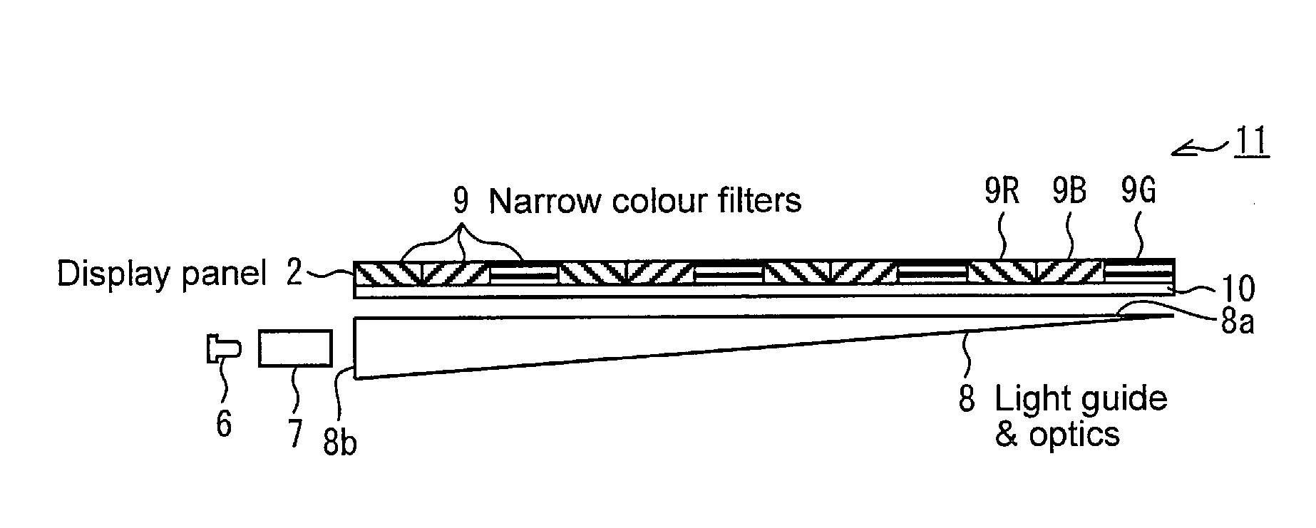
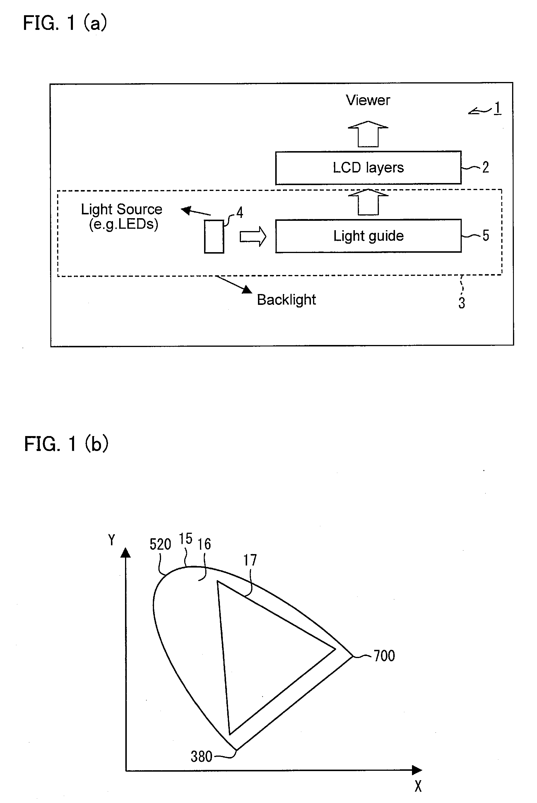
[0084]FIG. 3 is a schematic sectional view of a display 11 according to an embodiment of the present invention. The display 11 comprises a light source (described in more detail below), and an image display panel 2 disposed in an optical path from the light source. The display panel 2 comprises an image display layer 10 such as, for example, a liquid crystal layer. Components such as substrates for supporting the image display layer, electrodes and drive circuitry for driving the image display layer, and alignment films for, in the case of a liquid crystal image display layer, aligning the liquid crystal layer have been omitted from FIG. 3 for clarity. In this embodiment the display layer 10 is a pixellated image display layer, in which individual regions (“pixels”) of the image display layer may be driven independently of other regions.

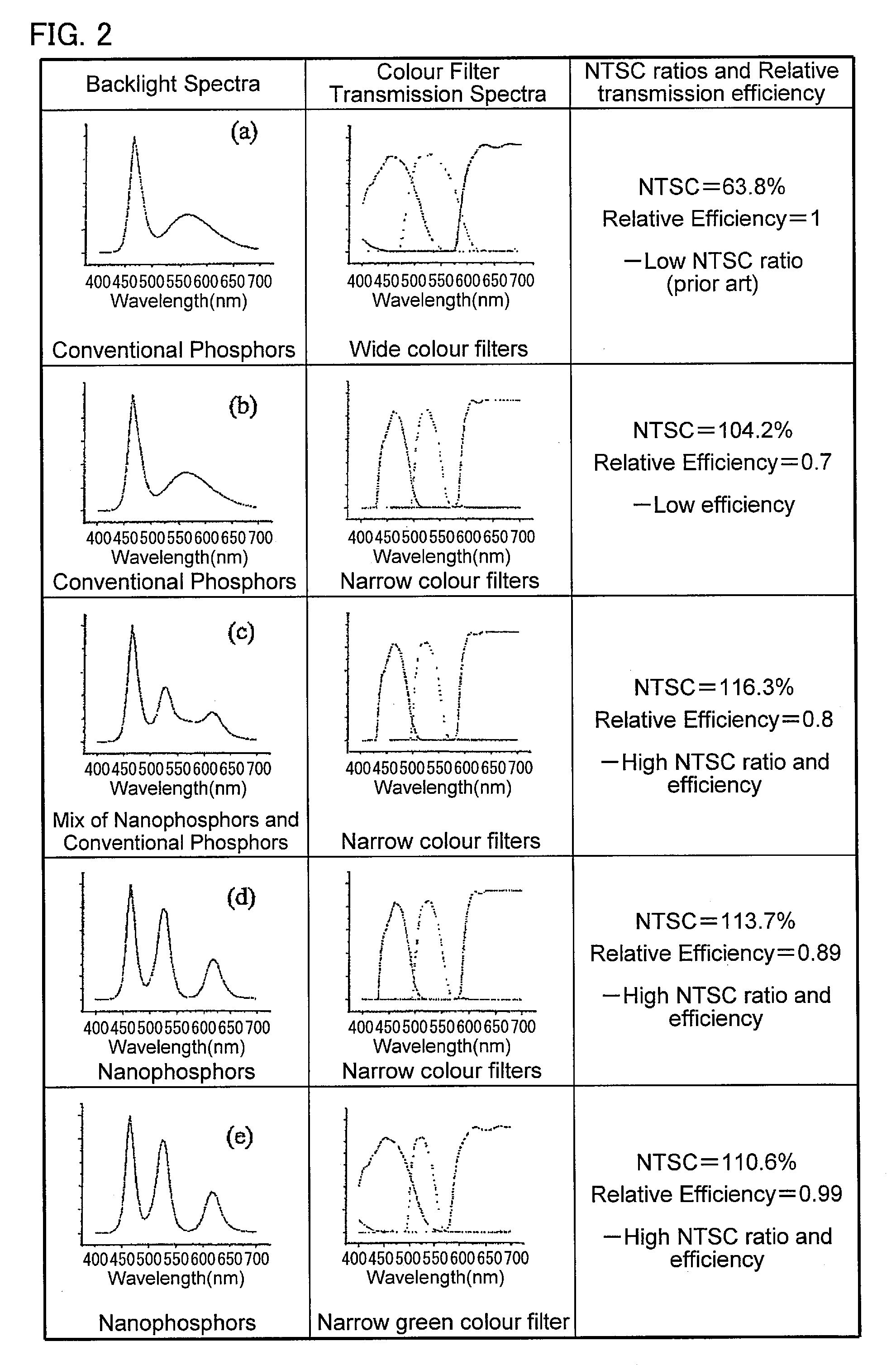
[0085]The display 11 is intended to provide a colour display, and the display panel 2 is therefore provided with colour filters 9. In the case of a ...


PUM


Abstract

A display comprises a light source and an image display panel disposed in an optical path from the light source. The light source comprises a primary light source for illuminating a re-emission material which comprises at least a first nanophosphor material for, when illuminated by light from the primary light source, re-emitting light in a first wavelength range different from the emission wavelength range of the primary light source. The image display panel comprises a first filter having a first narrow passband or a first narrow absorption band, the first narrow passband or first narrow absorption band being aligned or substantially aligned with the first wavelength range. The combination of a narrow wavelength range emitted by the first nanophosphor material and the narrow passband or narrow absorption band of the filter allows a display with high efficiency and a high NTSC ratio to be obtained.

Description

[0001]This Nonprovisional application claims priority under 35 U.S.C. § 119(a) on Patent Application No. 0619587.9 filed in U.K. on Oct. 4, 2006, the entire contents of which are hereby incorporated by reference.FIELD OF THE INVENTION[0002]The present invention relates to a display, for example such as Liquid Crystal Display (LCD), and in particular to a display using a backlight. Such displays are used in, for example, mobile phones, televisions, computer monitors etc.BACKGROUND OF THE INVENTION[0003]Many displays incorporate a transmissive display panel and a backlight for illuminating the display panel. FIG. 1(a) is a block schematic view of such a display 1. The display 1 comprises a transmissive display panel 2, for example a transmissive liquid crystal display panel, a light source 4 and a light guide 5. The light source 4 and the light guide 5 together comprise a backlight 3. In use, the display panel 2 is illuminated by the backlight 3 such that an image displayed on the dis...

Claims


Application Information

Patent Timeline
Patent Type & Authority Applications(United States)
IPC IPC(8): F21V9/08F21V9/16
CPCB82Y20/00G02F1/133514G02F2202/36G02F2001/133614G02F2202/046G02F1/133603G02F1/133614
Inventor ROSHAN, RAKESHTAYLOR, PETER NEILMONTGOMERY, DAVID JAMES
Owner SHARP KK
Why Eureka
Try Eureka