
Structure and manufacturing method of a chip scale package
a scale package and manufacturing method technology, applied in the direction of semiconductor devices, semiconductor/solid-state device details, electrical apparatus, etc., can solve the problems of significant degrading of chip performance, increasing negative impact on package performance, and increasing device density and device complexity, so as to improve the electrical performance of the device, shorten the interconnection, and cost-effective
- Summary
- Abstract
- Description
- Claims
- Application Information
AI Technical Summary
Benefits of technology
Problems solved by technology
Method used
Image

Examples
Embodiment Construction
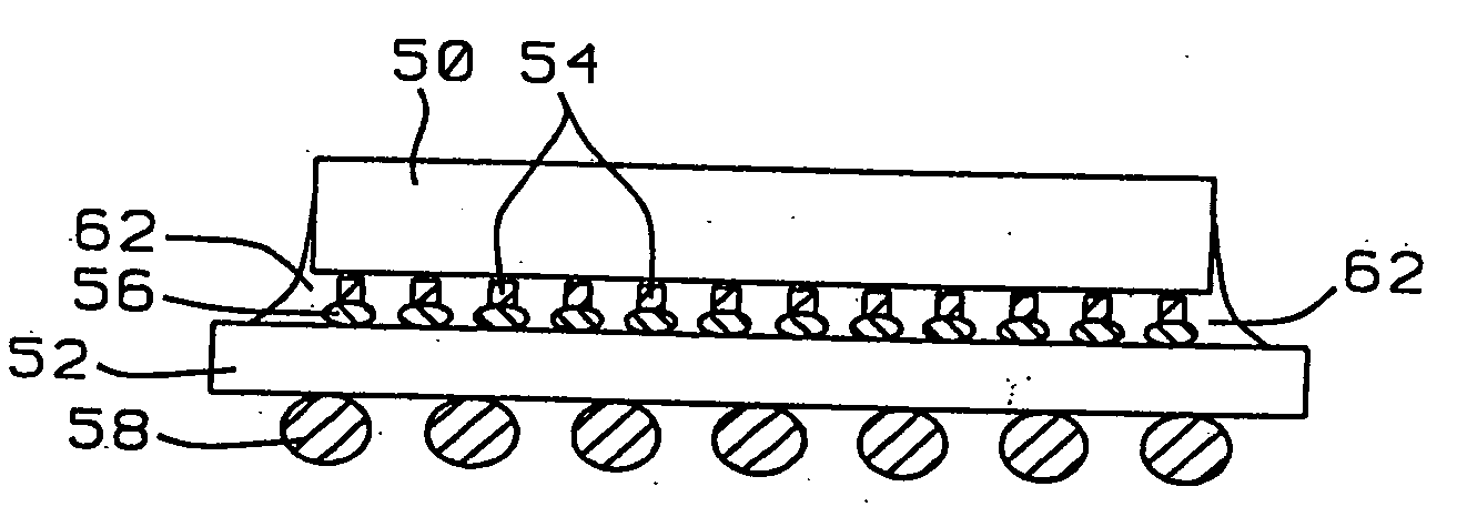
[0034] The above stated objective of improving chip accessibility during testing of the device, thus eliminating the need for special test fixtures, can further be highlighted as follows. The disclosed method of the invention, using Chip Scale Packaging (CSP), can control the cost of testing CSP devices by keeping the same body size of the chip and by using the same size substrate. For conventional CSP packages, the chip may have different body sizes, which imposes the requirement of different size test fixtures. With the continued reduction of the size of semiconductor devices, additional and varying device sizes are expected to be used. This would result in ever increasing costs for back-end testing of the devices in a production environment. The invention provides a method where these additional back-end testing costs can be avoided.
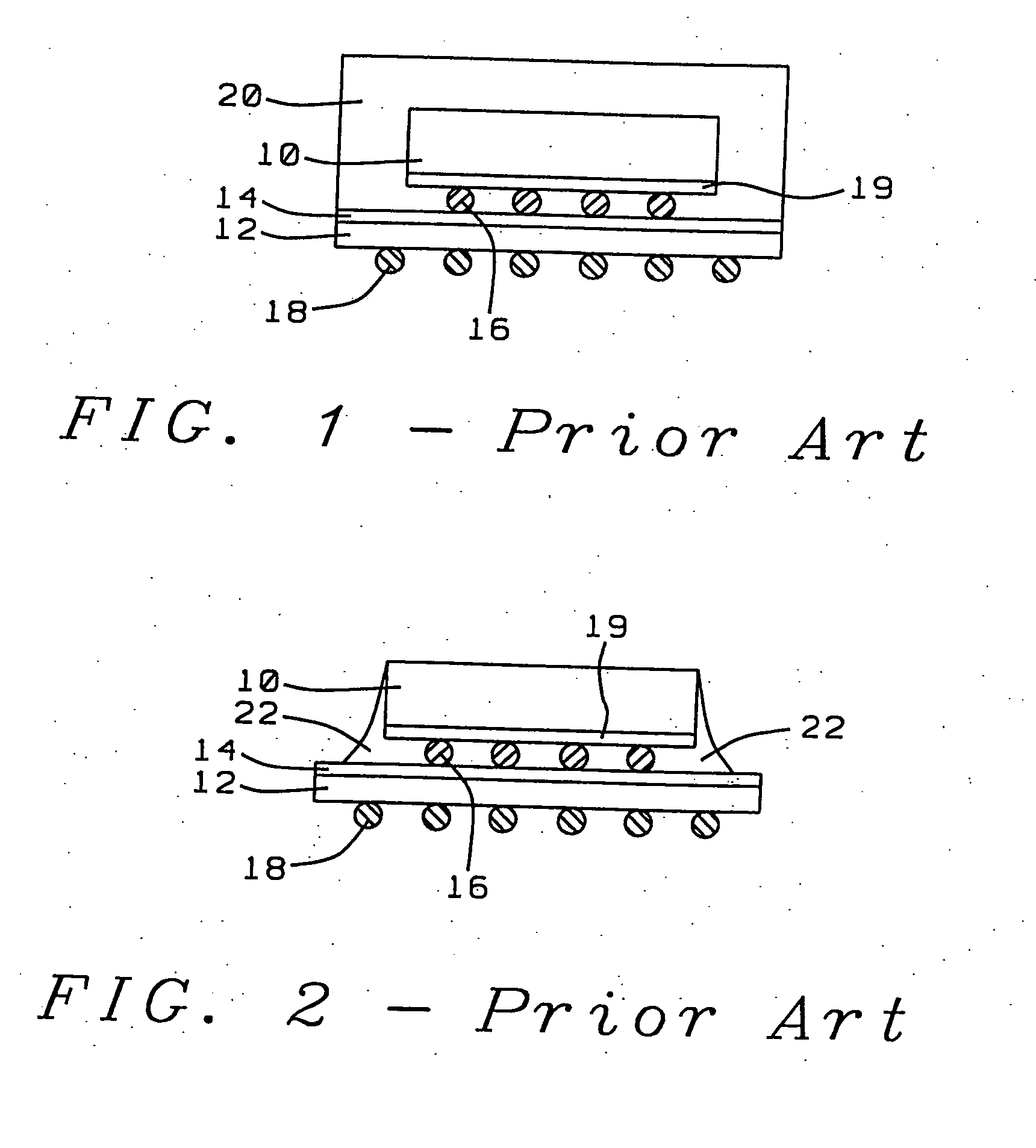
[0035] Referring now to FIG. 1, there is shown a cross section of a typical flip chip package with the semiconductor device being encapsulated in a ...
PUM
 Abstract
Description
Claims
Application Information