Method of manufacturing semiconductor laser for communication, semiconductor laser for communication and optical transmission module

a semiconductor laser and communication technology, applied in semiconductor lasers, semiconductor/solid-state device testing/measurement, instruments, etc., can solve the problems of inability to fully explain the failure mode of communication lasers using active materials with relatively many crystal defects, and no thorough study of screening test conditions included in the manufacturing process of ingaalas lasers, etc., to achieve high-reliability communication lasers

Active Publication Date: 2008-04-17
LUMENTUM JAPAN INC
View PDF4 Cites 10 Cited by
  • Summary
  • Abstract
  • Description
  • Claims
  • Application Information

AI Technical Summary

Benefits of technology

[0006] The material InGaAlAs for active layers, which is described in Paoletti et al., has a short history as a communication laser. Further there has been known that InGaAlAs has more crystal defects than InGaAsP. In addition, the failure mode of communication lasers using active materials with relatively many crystal defects has not been perfectly explained. For this reason, no thorough study has been done on the screening test conditi...

Problems solved by technology

In addition, the failure mode of communication lasers using active materials with relatively many crystal defects has not been perfectly exp...

Method used


Image

  • Method of manufacturing semiconductor laser for communication, semiconductor laser for communication and optical transmission module
  • Method of manufacturing semiconductor laser for communication, semiconductor laser for communication and optical transmission module
  • Method of manufacturing semiconductor laser for communication, semiconductor laser for communication and optical transmission module

Examples


embodiment 1

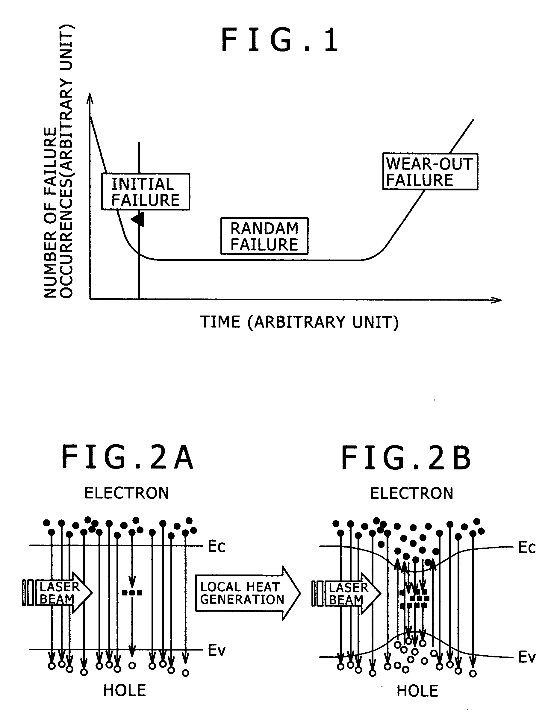
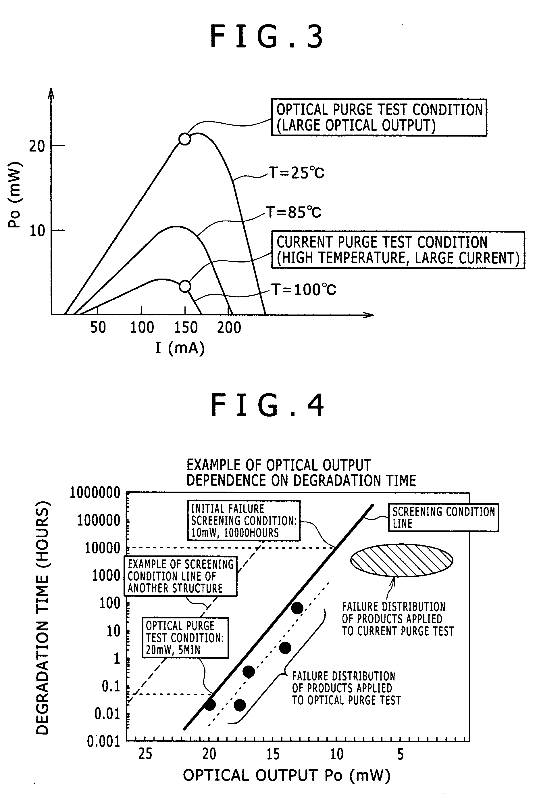
[0024] A first embodiment will be described with reference to FIGS. 2 to 8. Here, FIG. 2 is a view illustrating an initial failure mode due to the amount of optical output. FIG. 3 is a view illustrating the relation between the input power and the optical output (I-L characteristic) with temperature as a parameter. FIG. 4 is a view illustrating optical output dependence on optical degradation time. FIG. 5 is a cross-sectional view of a semiconductor laser in an optical axis direction. FIG. 6 is a perspective partial cross-sectional view of the semiconductor laser in an optical axis direction. FIG. 7 includes views illustrating a screening step of a semiconductor laser diode. FIG. 8 is a functional block diagram of an optical transmission module.

[0025] In FIG. 2, in a semiconductor laser using InGaAlAs as an active layer material, the nonradiative recombination and energy bandwidth reduction, or the positive feedback phenomenon of optical absorption, occurs through the interband tra...

embodiment 2

[0039] Referring to FIGS. 9, 10 and FIG. 7, a description will be made of a case in which the above described screening step was applied to the manufacturing process of a buried-heterostructure Fabry-Perot semiconductor laser diode for a wavelength of 1.3 μm band. Here, FIG. 9 is across-sectional view of a semiconductor laser in an optical axis direction. FIG. 10 is a perspective partial cross-sectional view of the semiconductor laser in an optical axis direction.

[0040] In FIG. 9, a buffer layer 201 (n-type InP, 1.5E18 cmˆ-3, 0.5 μm), an optical guide layer 202 (n-type InGaAlAs layer, 2E18 cmˆ-3, 0.1 μm), a multiple quantum well active layer 203 (well / barrier of InGaAlAs: 7 cycles, thickness 0.21 μm), an optical guide layer 204 (p-type InGaAlAs, 3E17 cmˆ-3, 0.1 μm)), an InAlAs clad layer 205 (p-type InAlAs, 8E17 cmˆ-3, 0.1 μm), an InP clad layer 209 (p-type InP, 1E18 cmˆ-3, 1.4 μm), and a contact layer 210 (p-type InGaAs, 1E19 cmˆ-3, 0.15 μm) were crystal grown sequentially on an I...

embodiment 3

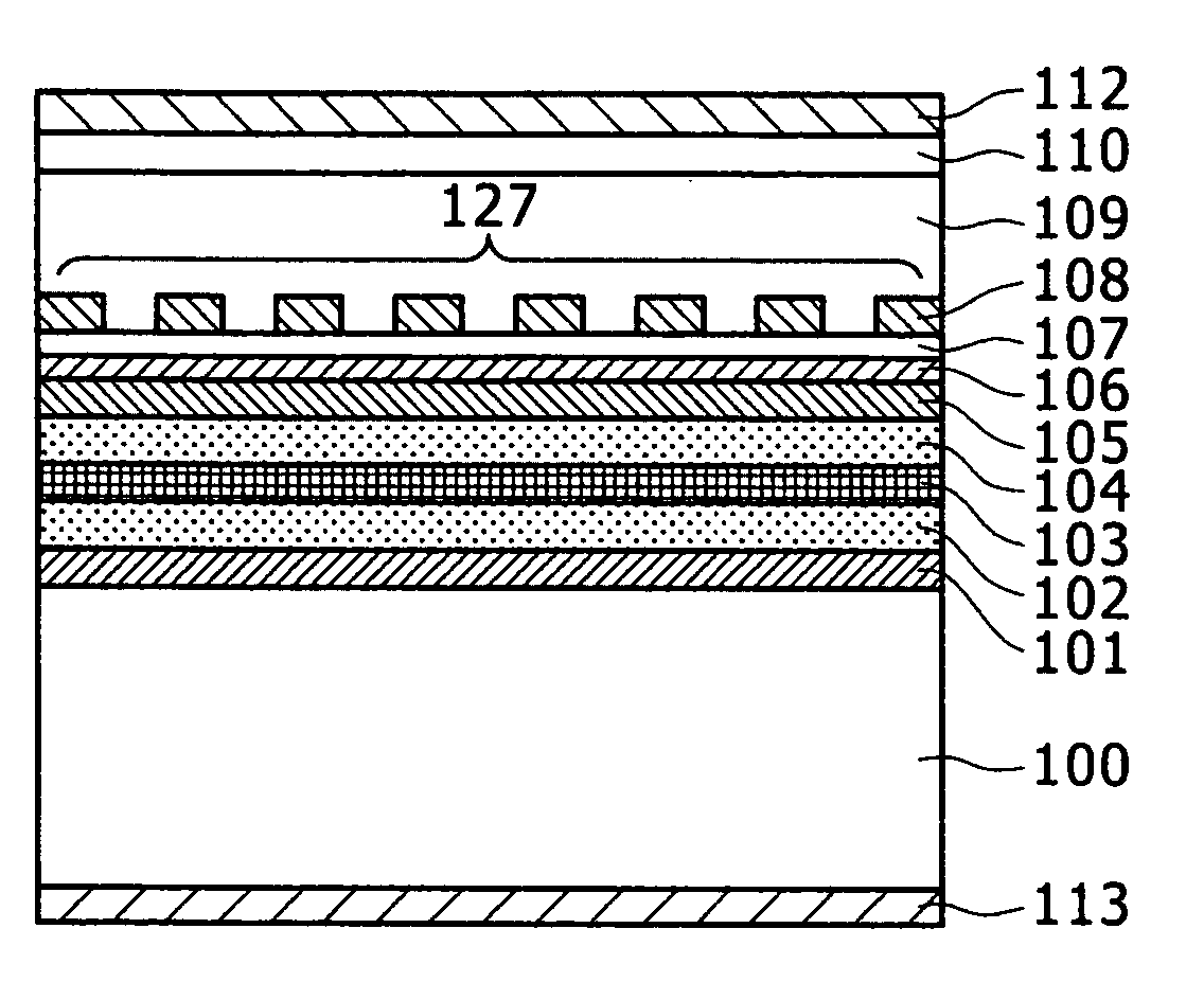
[0044] Referring to FIGS. 11, 12 and FIG. 7, a description will be made of the manufacturing process of a surface emitting semiconductor laser diode for a wavelength of 1.3 m band. FIG. 11 is a cross-sectional view of a surface emitting semiconductor laser. FIG. 12 is a perspective partial cross-sectional view of the surface emitting semiconductor laser in an optical axis direction.

[0045] As shown in FIG. 11, a buffer layer 302 (n-type InP layer, 1E18 cmˆ-3, 0.2 μm), a semiconductor reflection mirror 303 (n-type InAlAs / InGaAlAs layer, 1E18 cmˆ-3, 42-cycle structure of λ / 4 film thickness each), a lower contact layer 352 (n-type InP layer, 5E17 cmˆ-3, 0.2 μm), a clad layer 353 (n-type InAlAs layer, 5E17 cmˆ-3, 0.2 μm), an MQW layer 354 (well / barrier of InGaAlAs: 7 cycles, thickness 0.2 μm), a clad layer 355 (p-type InAlAs layer, 5E17 cmˆ-3, 0.7 μm), and a tunnel junction layer 356 (p+-InGaAlAs / n+InGaAs layer, 3E19 cmˆ-3, 20 nm / 12 nm) were crystal grown sequentially on an InP substrat...


PUM


Abstract

Some semiconductor lasers have an initial failure mode that is advanced as the amount of optical power therein, namely, the amount of optical output observed from the outside increases in almost independent of the temperature. The initial failure mode that is advanced as the amount of optical output increases is not sufficiently screened, so that the initial failure rate is somewhat higher than that of the semiconductor laser having the conventional active layer material. It is effective to introduce a test with large optical output at lower temperature than average operating temperature such as room temperature, during the manufacturing process. This helps to eliminate elements having the initial failure mode that is advanced as the amount optical output increases, thereby to extend the expected life of the laser diodes.

Description

CLAIM OF PRIORITY [0001] The present application claims priority from Japanese patent application serial no. 2006-225153, filed on Aug. 22, 2006, the content of which is hereby incorporated by reference into this application. BACKGROUND OF THE INVENTION [0002] The present invention relates to a method of manufacturing a semiconductor laser for communication, a semiconductor laser for communication and an optical transmission module, and more particularly to a method of manufacturing a semiconductor laser for communication with excellent reliability, a semiconductor laser for communication and an optical transmission module. [0003] As represented by a bathtub curve shown in FIG. 1, the failure mode of a product is generally classified into three types, namely an initial failure, a random failure, and a wear-out failure. The meaning of performing a screening test is to remove initial failure products of a semiconductor laser in short times, and to input products in a state of having a...

Claims


Application Information

Patent Timeline
IPC IPC(8): H01S5/00H01L21/66G01R31/26H01S5/12H01S5/343
CPCB82Y20/00H01S5/0021H01S5/12H01S5/343H01S5/18369H01S5/2231H01S5/3095H01S5/18308H01S5/00
Inventor KAMIYAMA, HIROYUKIMUKAIKUBO, MASARUINOUE, HIROAKIKITAHARA, CHIYUKI
Owner LUMENTUM JAPAN INC
Why Eureka
Try Eureka