Silicon Nitride Layer for Light Emitting Device, Light Emitting Device Using the Same, and Method of Forming Silicon Nitride Layer for Light Emitting Device

Inactive Publication Date: 2008-04-24
ELECTRONICS & TELECOMM RES INST
View PDF4 Cites 2 Cited by
  • Summary
  • Abstract
  • Description
  • Claims
  • Application Information

AI Technical Summary

Benefits of technology

[0009] The present invention is directed to a silicon nitride layer for a light emitting device, which is obtained in rela

Problems solved by technology

The above-described method involves additional processes and takes much time.
Also, problems caused by the high-temperature annealing process remain unsolved.
For these reasons, it is difficult to directly apply conventional semiconductor processes to the method.
Moreover, in manufacturing a light emitting device using silicon oxide, it is required to form a matrix or barrier to a very small thickness because of a high application voltage.

Method used


Image

  • Silicon Nitride Layer for Light Emitting Device, Light Emitting Device Using the Same, and Method of Forming Silicon Nitride Layer for Light Emitting Device
  • Silicon Nitride Layer for Light Emitting Device, Light Emitting Device Using the Same, and Method of Forming Silicon Nitride Layer for Light Emitting Device
  • Silicon Nitride Layer for Light Emitting Device, Light Emitting Device Using the Same, and Method of Forming Silicon Nitride Layer for Light Emitting Device

Examples


embodiment 1

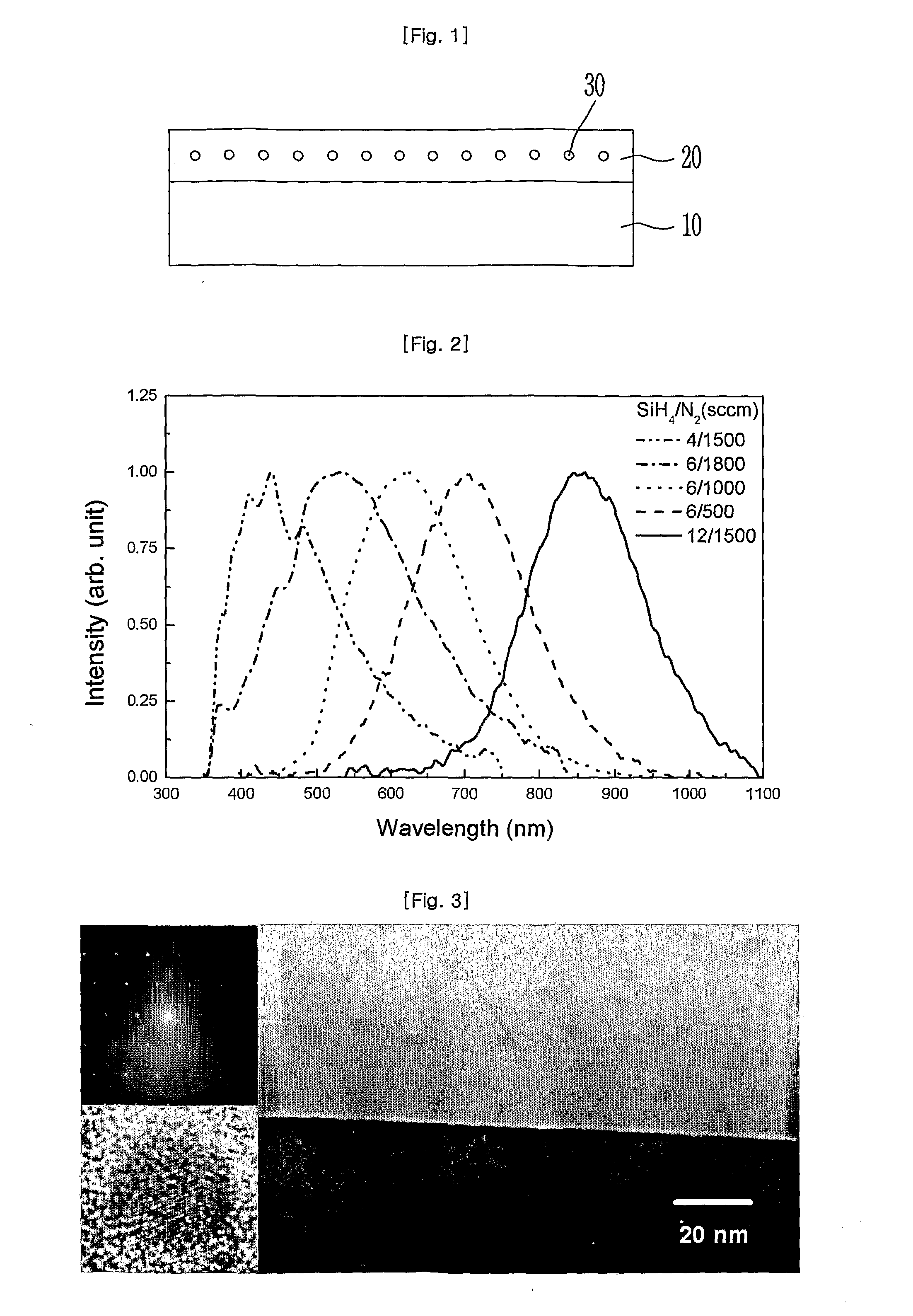
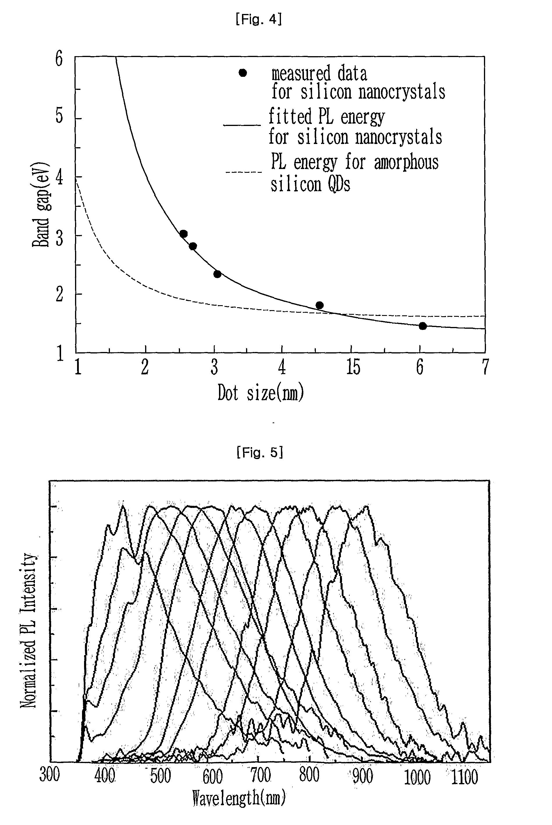
[0030]FIG. 1 is a cross-sectional view illustrating a process of forming a silicon nitride layer for a light emitting device according to an exemplary embodiment of the present invention.

[0031] Referring to FIG. 1, a silicon nitride matrix 20 is formed on a substrate 10, and silicon nanocrystals 30 are formed in the silicon nitride matrix 20.

[0032] The substrate 10 may be, but not limited thereto, a semiconductor substrate such as a silicon (Si) substrate and a germanium (Ge) substrate, a compound semiconductor substrate such as a SiGe substrate, a SiC substrate, a GaAs substrate, and an InGaAs substrate, or an insulating substrate such as a glass substrate, a sapphire substrate, a quartz substrate, and a resin substrate. However, when a silicon nitride layer is formed on a silicon substrate, the silicon substrate has better lattice match. Meanwhile, good lattice match can also be obtained when an additional silicon layer is formed on a substrate other than a silicon substrate and...

embodiment 2

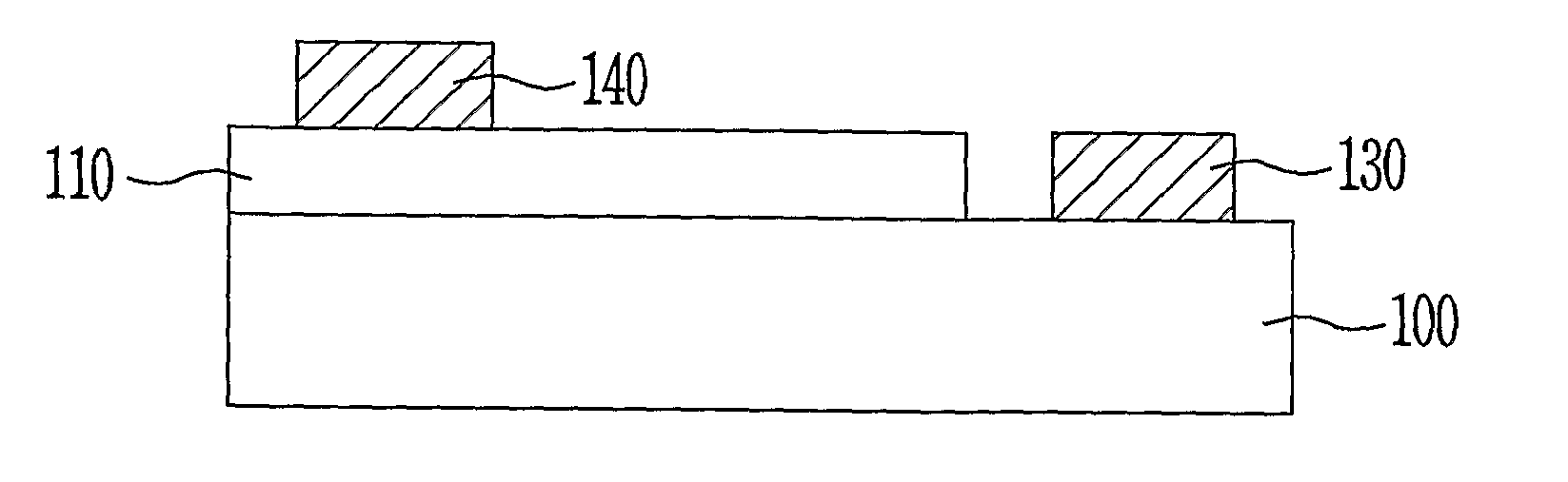
[0050]FIG. 6 is a cross sectional view of a silicon light emitting device according to another exemplary embodiment of the present invention.

[0051] Referring to FIG. 6, a silicon emission layer 110 is formed on a predetermined region of a substrate 100, a p-type electrode 120 is formed on another predetermined region of the substrate 100 where the silicon emission layer 110 is not formed. Preferably, the substrate 100 is a p-type silicon substrate.

[0052] The silicon emission layer 110 may be formed using the above-described silicon nitride layer for the light emitting device according to the first embodiment and includes a silicon nitride matrix and silicon nanocrystals formed in the silicon nitride matrix.

[0053] Meanwhile, an n-type electrode 140 is formed on a predetermined region of the silicon emission layer 110. An n-type doping process may be performed using, for example, a P-based dopant, and a p-type doping process may be performed using, for example, a B-based dopant.

[0...


PUM

PropertyMeasurementUnit
Fractionaaaaaaaaaa
Thicknessaaaaaaaaaa
Diameteraaaaaaaaaa

Abstract

Provided are a silicon nitride layer for a light emitting device, light emitting device using the same, and method of forming the silicon nitride layer for the light emitting device. The silicon nitride layer of the light emitting device includes a silicon nitride matrix and silicon nanocrystals formed in the silicon nitride matrix. A light emitting device manufactured by the silicon nitride layer has a good luminous efficiency and emits light in the visible region including the short-wavelength blue / violet region and the near infrared region.

Description

BACKGROUND ART [0001] 1. Field of the Invention [0002] The present invention relates to a silicon nitride layer for a light emitting device, light emitting device using the same, and method of forming the silicon nitride layer for the light emitting device, and more specifically, to a silicon nitride layer for a light emitting device, which includes a silicon nitride matrix and silicon nanocrystals formed in the silicon nitride matrix. [0003] 2. Description of Related Art [0004] In order to obtain a light emitting effect using silicon as an indirect bandgap semiconductor, it is necessary to provoke a quantum confinement effect due to fine structures (Refer to Light Emission in Silicon: From Physics to Devices, edited by D. J. Lockwood (Academic Press, San Diego, 1998), Chap. 1). [0005] The quantum confinement effect involves forming fine crystalline or amorphous silicon structures having a size of several nm or less (e.g., quantum wells, quantum wires, and quantum dots) using a matr...

Claims


Application Information

Patent Timeline
IPC IPC(8): H01L33/00H01L21/36H01L33/34H01L33/40
CPCC23C16/30C23C16/345H01L33/34H01L33/18H01L33/08Y10S977/773
Inventor KIM, TAE YOUBPARK, NAE MANKIM, KYUNG HYUNSUNG, GUN YONG
Owner ELECTRONICS & TELECOMM RES INST
Why Eureka
Try Eureka