Oxidation apparatus and method for semiconductor process

Active Publication Date: 2008-04-24
TOKYO ELECTRON LTD
View PDF17 Cites 10 Cited by
  • Summary
  • Abstract
  • Description
  • Claims
  • Application Information

AI Technical Summary

Benefits of technology

[0010]An object of the present invention is to provide an oxidation apparatus and method for a semiconductor

Problems solved by technology

In this respect, a film formed by wet oxidation under a normal pressure shows a high oxidation rate, but shows poor planar uniformity in film thicknes

Method used


Image

  • Oxidation apparatus and method for semiconductor process
  • Oxidation apparatus and method for semiconductor process
  • Oxidation apparatus and method for semiconductor process

Examples


Example

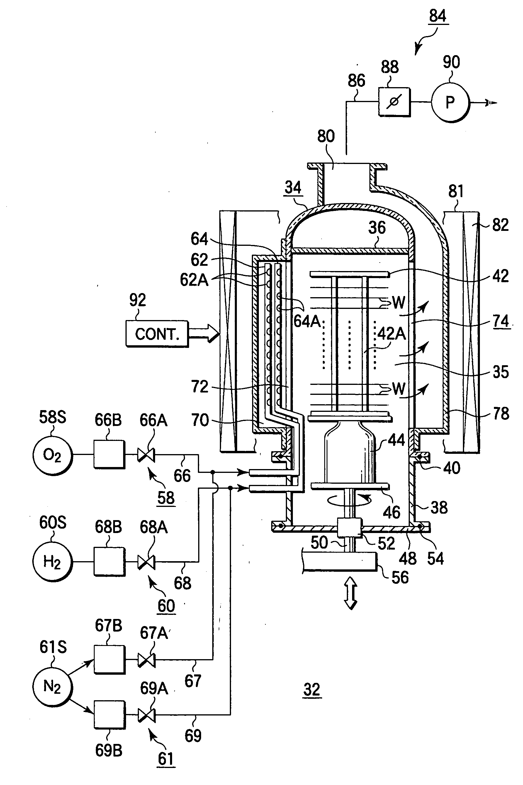
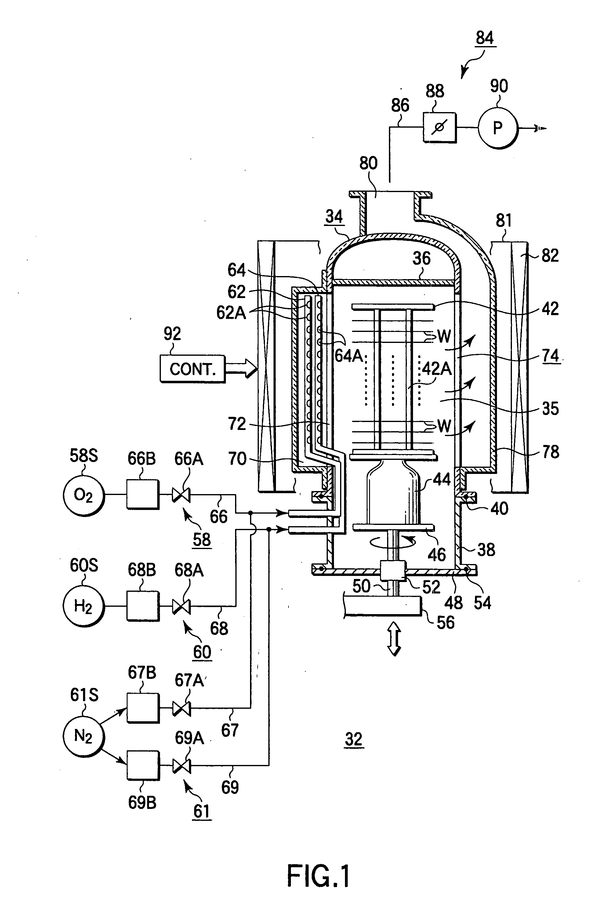
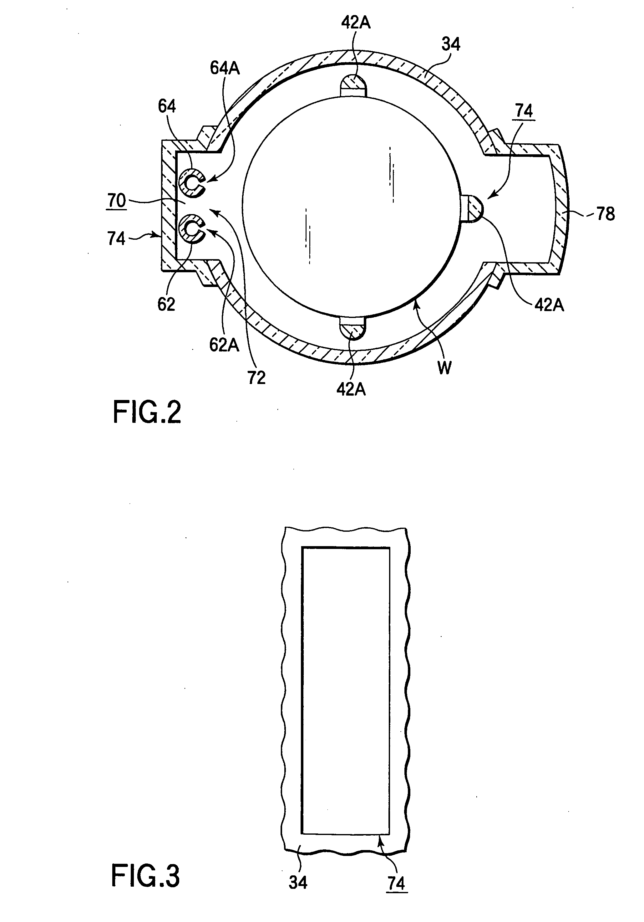
[0028]In the process of developing the present invention, the inventors studied problems of conventional techniques for semiconductor processes, in relation to a method for forming an oxide film by oxidation. As a result, the inventors have arrived at the findings given below.

[0029]In an oxidation method for oxidizing a wafer surface by causing H2 gas and O2 gas to react without each other under a low pressure, various activated species (radicals) generated by reactions have very high reactivity. In this case, oxidation proceeds without reference to the orientation of crystal planes exposed on the wafer surface, i.e., without dependency on the orientation of crystal planes. Consequently, ever where ragged patterns are present on the wafer surface, an oxide film is formed with a uniform film thickness along the surface of ragged patterns. Further, since radicals are very reactive, a film difficult to oxidize, i.e., an oxidation resistant film, such as a silicon nitridation film, can ...


PUM

PropertyMeasurementUnit
Temperatureaaaaaaaaaa
Pressureaaaaaaaaaa
Pressureaaaaaaaaaa

Abstract

An oxidation apparatus for a semiconductor process includes a gas supply system configured to supply an oxidizing gas and a deoxidizing gas to the process field of a process container through a gas supply port disposed adjacent to target substrates on one side of the process field. The gas supply port includes a plurality of gas spouting holes arrayed over a length corresponding to the process field in a vertical direction. A heater is disposed around the process container and configured to heat the process field. A control section is preset to perform control such that the oxidizing gas and the deoxidizing gas are caused to react with each other, thereby generating oxygen radicals and hydroxyl group radicals within the process field, and an oxidation process is performed on the surfaces of the target substrate by use of the oxygen radicals and the hydroxyl group radicals.

Description

BACKGROUND OF THE INVENTION[0001]1. Field of the Invention[0002]The present invention relates to an oxidation apparatus and method for a semiconductor process for oxidizing the surface of a target substrate, such as a semiconductor wafer. The term “semiconductor process” used herein includes various kinds of processes which are performed to manufacture a semiconductor device or a structure having wiring layers, electrodes, and the like to be connected to a semiconductor device, on a target substrate, such as a semiconductor wafer or a glass substrate used for an FPD (Flat Panel Display), e.g., an LCD (Liquid Crystal Display), by forming semiconductor layers, insulating layers, and conductive layers in predetermined patterns on the target substrate.[0003]2. Description of the Related Art[0004]In manufacturing semiconductor integrated circuits, a semiconductor substrate, such as a silicon wafer, is subjected to various processes, such as film formation, etching, oxidation, diffusion, ...

Claims


Application Information

Patent Timeline
IPC IPC(8): B01J19/00
CPCH01L21/02238H01L21/67109H01L21/31662H01L21/02255
Inventor HASEBE, KAZUHIDEFUJITA, TAKEHIKONAKAJIMA, SHIGERUOGAWA, JUN
Owner TOKYO ELECTRON LTD
Why Eureka
Try Eureka