Manufacturing method of semiconductor device and semiconductor device

a manufacturing method and technology of semiconductor devices, applied in semiconductor devices, semiconductor/solid-state device details, electrical devices, etc., can solve the problems of degrading the moisture resistance of the insulating film, the flatness of the surface the deformation of the insulating film, so as to improve the moisture resistance of the semiconductor device and the high moisture resistance

a manufacturing method and technology of semiconductor devices, applied in semiconductor devices, semiconductor/solid-state device details, electrical devices, etc., can solve the problems of degrading the moisture resistance of the insulating film, the flatness of the surface the deformation of the insulating film, so as to improve the moisture resistance of the semiconductor device and the high moisture resistance

US20080099876A1Inactive Publication Date: 2008-05-01LAPIS SEMICON CO LTD

Image

  • Manufacturing method of semiconductor device and semiconductor device
  • Manufacturing method of semiconductor device and semiconductor device
  • Manufacturing method of semiconductor device and semiconductor device

Examples


first preferred embodiment

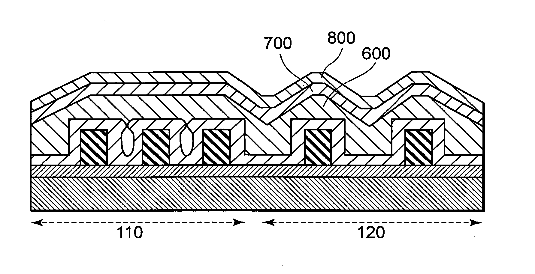
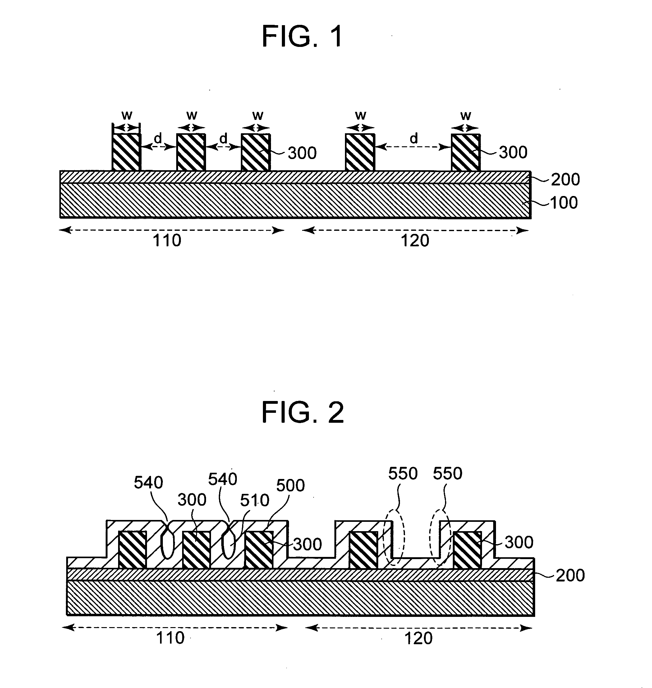
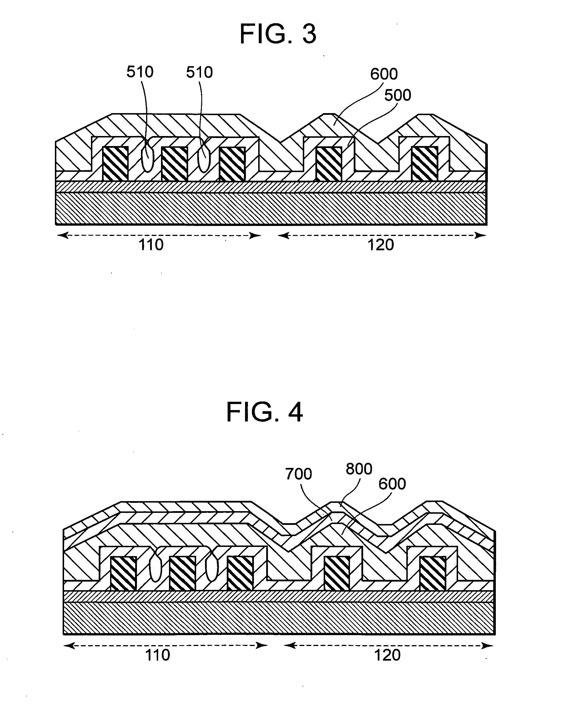
[0017]FIGS. 1 through 7 are process diagrams for describing a method for manufacturing a semiconductor device according to a first embodiment of the invention of the present application. Here, FIGS. 1 through 6 are sectional views of the semiconductor device.

[0018] In the first embodiment, a plurality of wirings 300 are formed adjacent to one another on a first insulating film 200 formed on a semiconductor substrate 100 as shown in FIG. 1.

[0019] The semiconductor substrate 100 is a silicon (Si) substrate. The first insulating film 200 is a silicon oxide (SiO2) film and is formed by a high density plasma CVD (Chemical Vapor Deposition) method. The wirings 300 has a stacked structure in which a titanium nitride (TiN) film, an aluminum-copper (AlCu) film and a titanium nitride (TiN) film are sequentially laminated on one another. The wirings 300 are obtained by stacking the above respective metal films on one another by a sputtering method and patterning the same.

[0020] In the prese...


PUM


Abstract

The present invention provides a method of manufacturing a semiconductor device, which comprises steps of forming a plurality of wirings on a first insulting film formed on a semiconductor substrate so as to adjoin one another, forming a second insulating film on the first insulating film by a plasma CVD method and covering the wirings with the second insulating film in such a manner that air gaps are formed between the respective adjacent wirings, forming a third insulating film on the second insulating film by a high density plasma CVD method, and forming a fourth insulating film high in moisture resistance on the third insulating film.

Description

BACKGROUND OF THE INVENTION [0001] The present invention relates to a method for manufacturing a semiconductor device, and particularly to a method for manufacturing a semiconductor device wherein air gaps are formed between wirings formed on a semiconductor substrate. [0002] There has heretofore been known a semiconductor device having air gaps provided between wirings with a view toward reducing capacitance between the wirings formed on a semiconductor substrate. [0003] A method of manufacturing the semiconductor device provided with the air gaps includes a step for forming wirings on a first insulating film formed on a semiconductor substrate, so as to adjoin one another, a step for forming a second insulating film on the first insulating film by a plasma CVD method and covering the wirings with the second insulating film such that the air gaps are formed between the adjacent wirings, and a step for forming a third insulating film high in moisture resistance on the second insulat...

Claims


Application Information

Patent Timeline
01 May 2008
Publication
US20080099876A1
IPC
H01L23/00; H01L21/4763
CPC
H01L21/7682; H01L21/76801
Inventors
SETO, MASARU