SOI-based inverse nanotaper optical detector

a technology of optical detectors and nano-tapers, applied in the direction of basic electric elements, electrical equipment, semiconductor devices, etc., can solve the problems of limiting the application of communication industry, affecting the performance of devices, and expensive and complicated integration of such devices on silicon surfaces, etc., to achieve the effect of easy and efficient implementation

Inactive Publication Date: 2008-05-08
SIOPTICAL INC +1
View PDF10 Cites 48 Cited by
  • Summary
  • Abstract
  • Description
  • Claims
  • Application Information

AI Technical Summary

Benefits of technology

[0016]The utilization of an inverse nanotaper coupling tip provides for efficient conversion of the incoming lightwave signal, where the dimensions of the tip are defined to capture the majority of the lightwave signal as it enters the SOI structure. Inasmuch as the photodetecting device is formed as an integral part of the nanotaper itself, the distance along which the signal must propagate prior to entering the photodetecting device is substantially reduced.
[0017]The arrangement of the present invention may be used as a conventional photodetector, where most (if not all) of the incoming lightwave signal is converted into an electrical output (in one case, by truncating the inverse nanotaper coupler at the termination of the tapered region). Alternatively, the inverse nanotaper photodetector may be configured as an in-line device to convert any desired fraction of the incoming lightwave signal into an electrical signal, allowing the remaining optical signal to continue to propagate along an optical waveguide contiguous with the inverse nanotaper coupling waveguide. Various types of feedback and control arrangements may desire the ability to measure / monitor only a portion of the received light signal by electrical means, and this particular arrangement of the present invention allows for this monitoring to be implemented easily and efficiently.

Problems solved by technology

The majority of the InGaAs-based detectors are normal incidence detectors and, as a result, the integration of such devices on silicon surfaces is expensive and complicated.
Additionally, integration of high-speed InGaAs detectors requires special optics to focus light into a small active area, which has been found to have a deleterious effect on device performance.
Germanium detectors exhibit a higher dark current than InGaAs-based detectors, which limit their application in the communication industry.
While SOI-based photodetectors of the type as shown in FIG. 1 represent a significant advance in the state of the art, problems arise when the input lightwave signal exhibits random, unknown polarization.

Method used


Image

  • SOI-based inverse nanotaper optical detector
  • SOI-based inverse nanotaper optical detector
  • SOI-based inverse nanotaper optical detector

Examples


Embodiment Construction

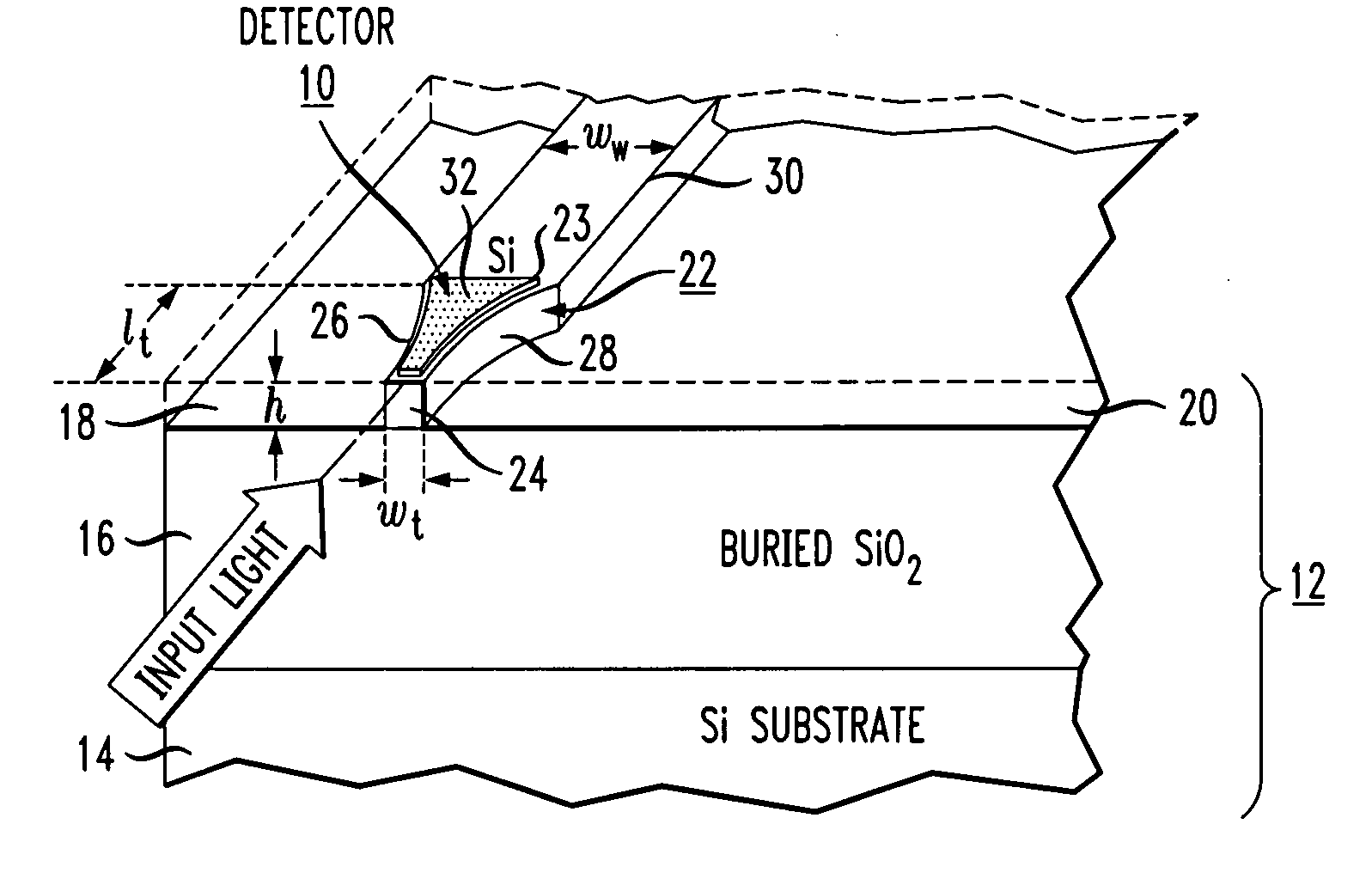
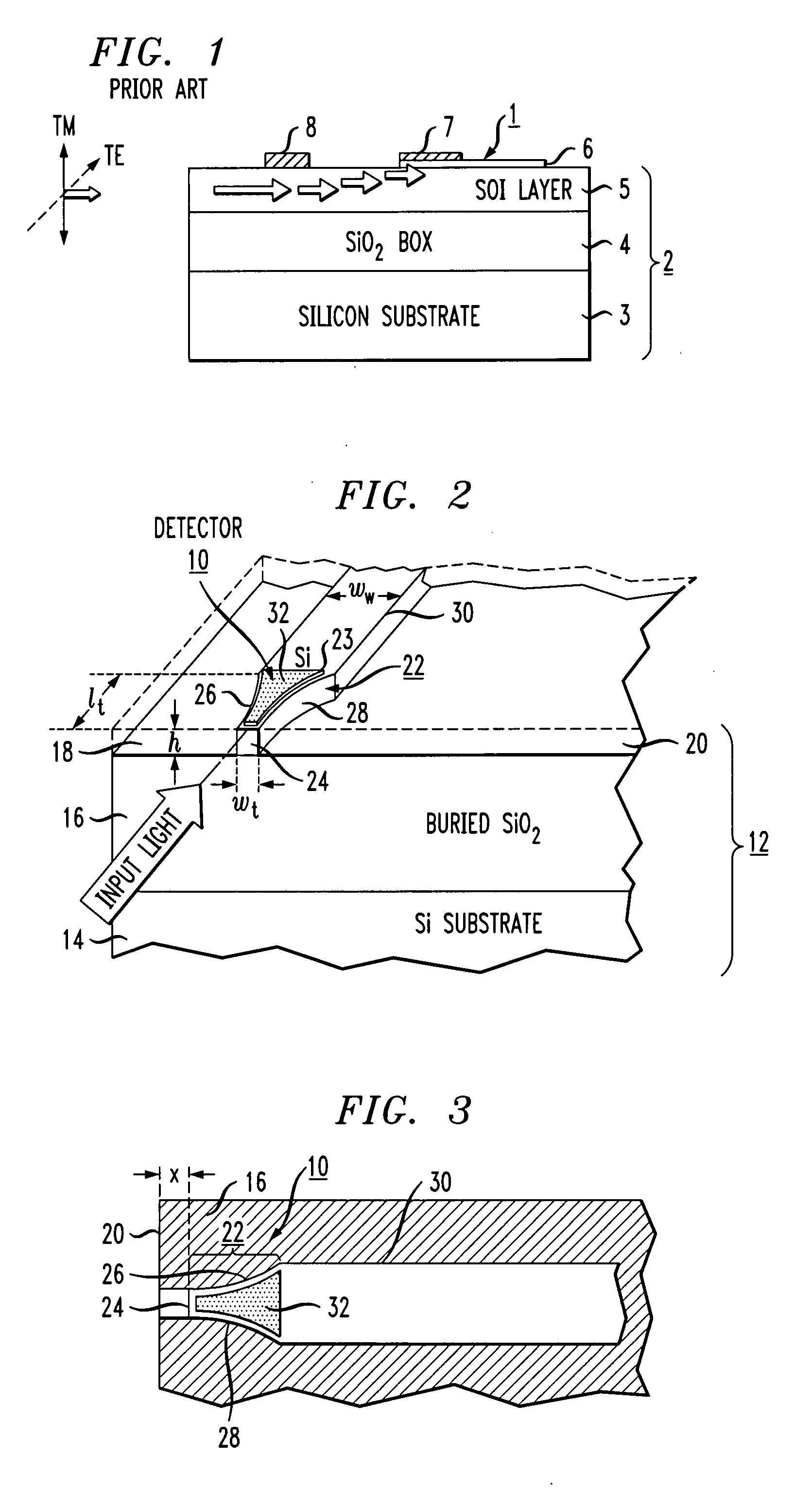
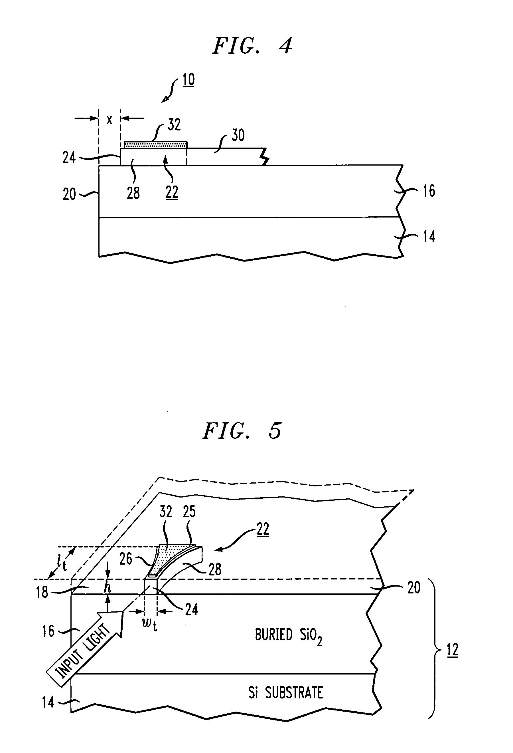
[0030]FIG. 2 is an isometric view of an exemplary inverse nanotaper photodetector 10 formed in accordance with the present invention, where FIG. 3 is a top view and FIG. 4 is a side view of the same embodiment. As shown, inverse nanotaper photodetector 10 is disposed on an SOI structure 12, where structure 12 includes a silicon substrate 14, buried oxide layer 16 and a silicon surface layer 18 (hereinafter referred to as “SOI layer 18”). The isometric view of FIG. 2 is a view along an endface 20 of SOI structure 12, with the incoming lightwave signal approaching detector 10 in the manner shown.

[0031]Detector 10 comprises an inverse nanotaper coupling waveguide 22, which is formed as an etched portion of SOI layer 18, beginning at endface 20. Waveguide 22 is formed to exhibit a predetermined height h (which may simply be the thickness of SOI layer 18, in most cases less than one micron) and a relatively narrow tip width wt at waveguide endface 24 (also referred to as “tip 24”). Waveg...


PUM


Abstract

A photodetector integrated within a silicon-on-insulator (SOI) structure is formed directly upon an inverse nanotaper endface coupling region to reduce polarization sensitivity at the detector's input. The photodetector may be germanium-based PN (PIN) junction photodetector, a SiGe photodetector, a metal / silicon Schottky barrier photodetector, or any other suitable silicon-based photodetector. The inverse nanotaper photodetector may also be formed as an in-line monitoring device, converting only a portion of the in-coupled optical signal and allowing for the remainder to thereafter propagate along an associated optical waveguide.

Description

CROSS-REFERENCE TO RELATED APPLICATION[0001]The present application claims the benefit of Provisional Application No. 60 / 813,936, filed Jun. 15, 2006.TECHNICAL FIELD[0002]The present invention is related to a photodetector arrangement for use with silicon-based opto-electronic arrangements and, more particularly, to an SOI-based photodetector integrated with an inverse nanotaper input coupler.DESCRIPTION OF THE PRIOR ART[0003]Conversion of photons to electrons is essential for the successful integration of microphotonics with microelectronics. InGaAs-based PIN photodetectors are commonly used for communication applications because of their high responsivity and speed. The majority of the InGaAs-based detectors are normal incidence detectors and, as a result, the integration of such devices on silicon surfaces is expensive and complicated. Additionally, integration of high-speed InGaAs detectors requires special optics to focus light into a small active area, which has been found to ...

Claims


Application Information

Patent Timeline
Patent Type & Authority Applications(United States)
IPC IPC(8): H01L31/0232
CPCH01L31/03529Y02E10/50H01L31/103
Inventor PIEDE, DAVIDPATEL, VIPULKUMARGHIRON, MARGARETGOTHOSKAR, PRAKASHMONTGOMERY, ROBERT KEITH
Owner SIOPTICAL INC
Why Eureka
Try Eureka