Susceptor For Vapor-Phase Growth Reactor

a technology of vapor-phase growth and susceptor, which is applied in the direction of crystal growth process, chemically reactive gas, coating, etc., can solve the problems of temperature difference between a part facing through the through hole portion of the wafer and another part, and the non-defective rate is falling,

Inactive Publication Date: 2008-05-15
SUMCO CORP
View PDF4 Cites 181 Cited by
  • Summary
  • Abstract
  • Description
  • Claims
  • Application Information

AI Technical Summary

Benefits of technology

[0018]Namely, the fluid passage according to the present invention is not limited to the embodiment of providing holes on the susceptor structure, and the susceptor itself may be configured by combining a plurality of structures, forming a clearance by surfaces of two structures put together and using the same as a fluid passage. When applying such configuration as above to prevent irradiation of radiant heat from the heat source directly to the wafer back surface, one end of the clearance as a fluid passage formed between the first structure and second structure opens on the vertical wall positioned below the first pocket portion. As a result, the vertical wall becomes substantially perpendicular to the wafer back surface, so that irradiation of radiant heat from the heat source directly to the wafer back surface is prevented. Note that the other end of the fluid passage may open on the back surface of the susceptor or on the side surface of the susceptor.

Problems solved by technology

As a result, there arises a region where a dopant concentration becomes uncontrollable in the epitaxial layer, which leads to a decline of a non-defective rate.
However, when forming through holes on a wafer pocket of a susceptor, radiant heat from a heater, such as a halogen lamp, provided below the susceptor passes through the through hole portions to irradiate a back surface of a wafer and there arises a temperature difference between a part facing to the through hole portions of the wafer and other part.
Consequently, there has been a problem that unevenness of growth arises on the epitaxial layer and a back surface of the wafer.

Method used


Image

  • Susceptor For Vapor-Phase Growth Reactor
  • Susceptor For Vapor-Phase Growth Reactor
  • Susceptor For Vapor-Phase Growth Reactor

Examples


examples

[0056]Below, examples of the present invention will be explained by comparing with comparative examples to clarify the effects of the present invention.

[0057]As a unified condition of examples and comparative examples, a P+ type silicon monocrystal wafer having a diameter of 200 mm, a main surface in a surface direction of (100) and resistivity of 15 m Ω·cm was used to grow on the wafer surface a P type epitaxial film having a thickness of about 6 μm and resistivity of 10 Ω·cm at an epitaxial growth temperature of 1125° C. by performing hydrogen baking at 1150° C. for 20 seconds and supplying a mixed reaction gas obtained by diluting SiHCl3 as a silicon source and B2H6 as a boron-dopant source by a hydrogen gas into the vapor-phase growth reactor.

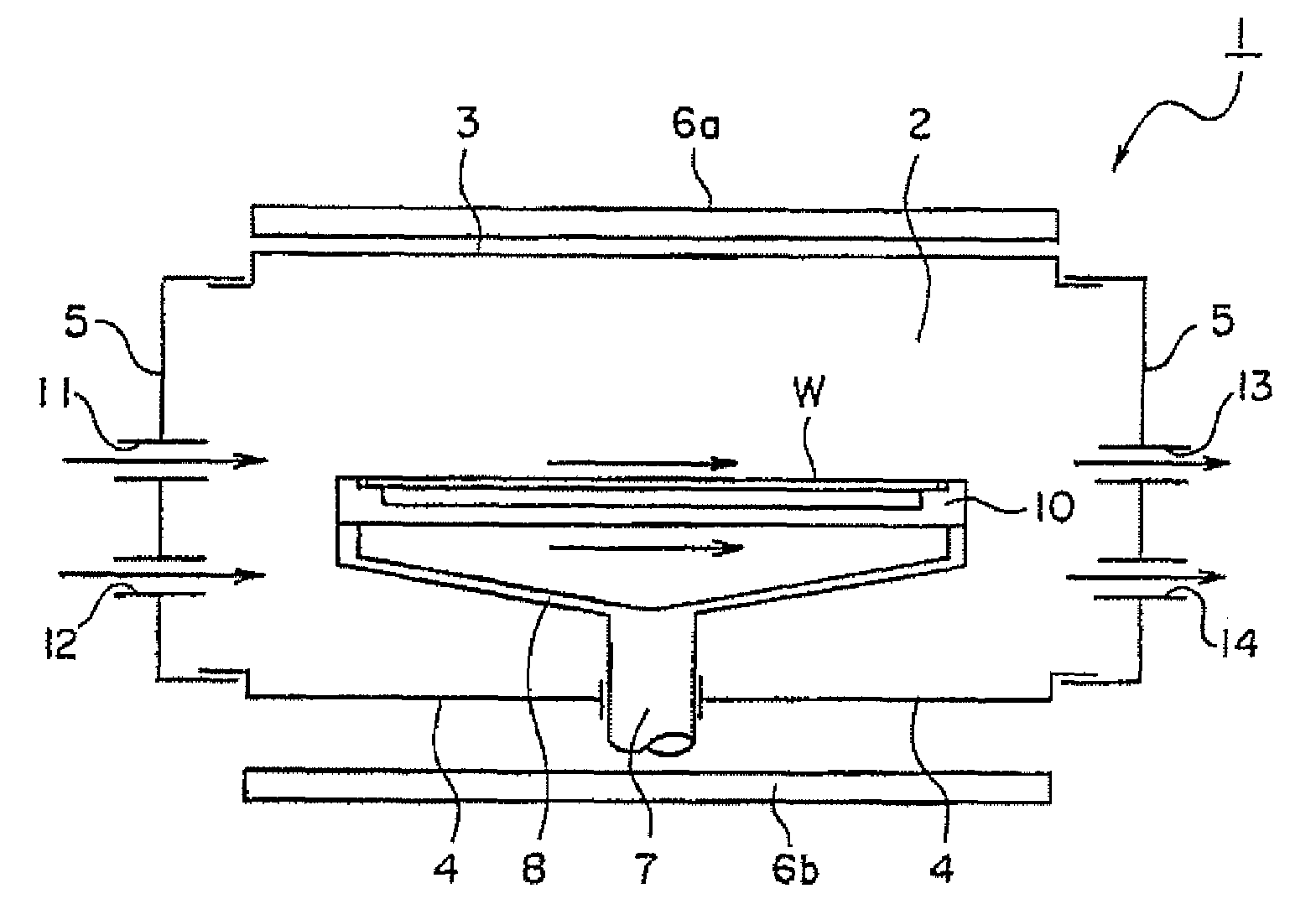
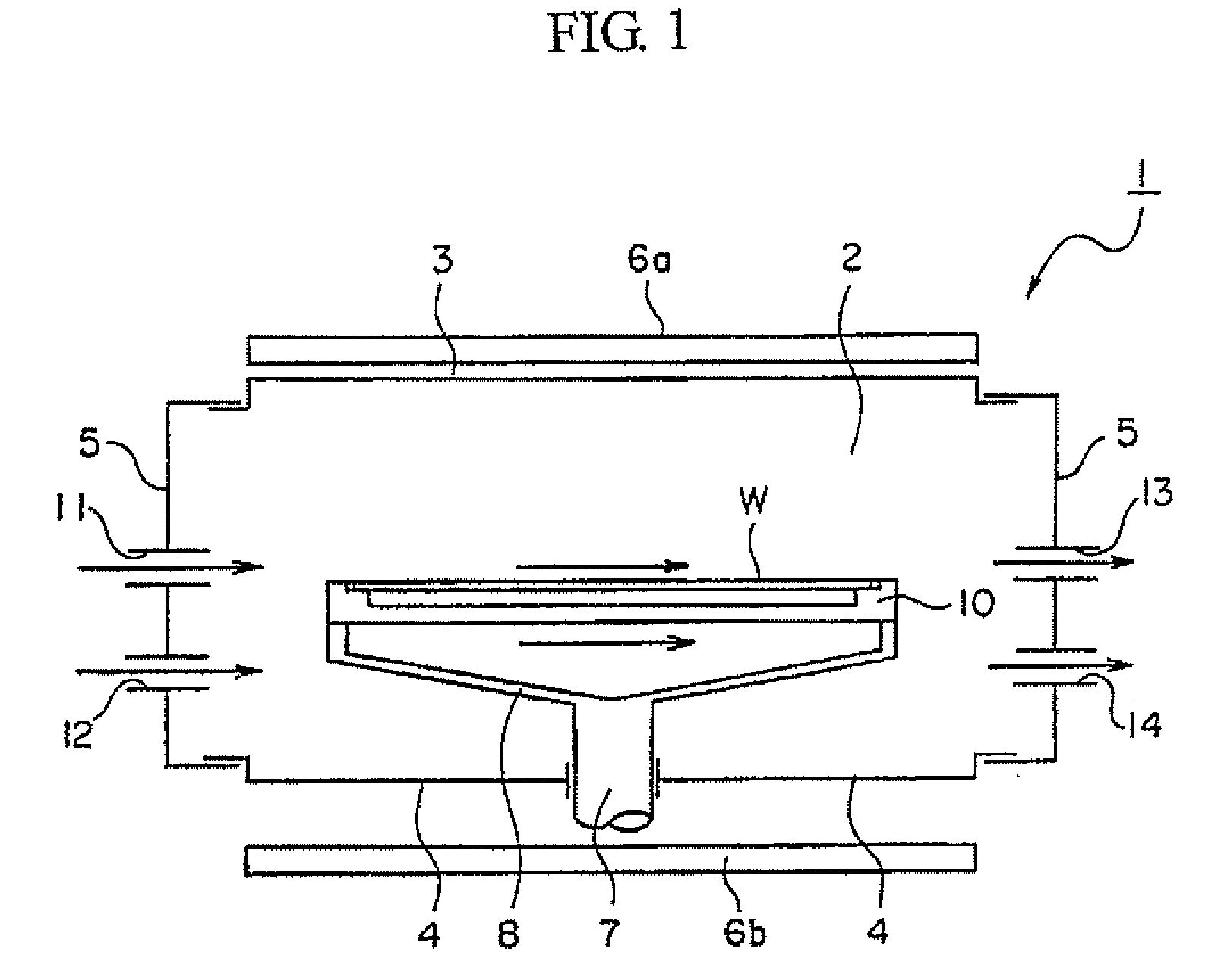
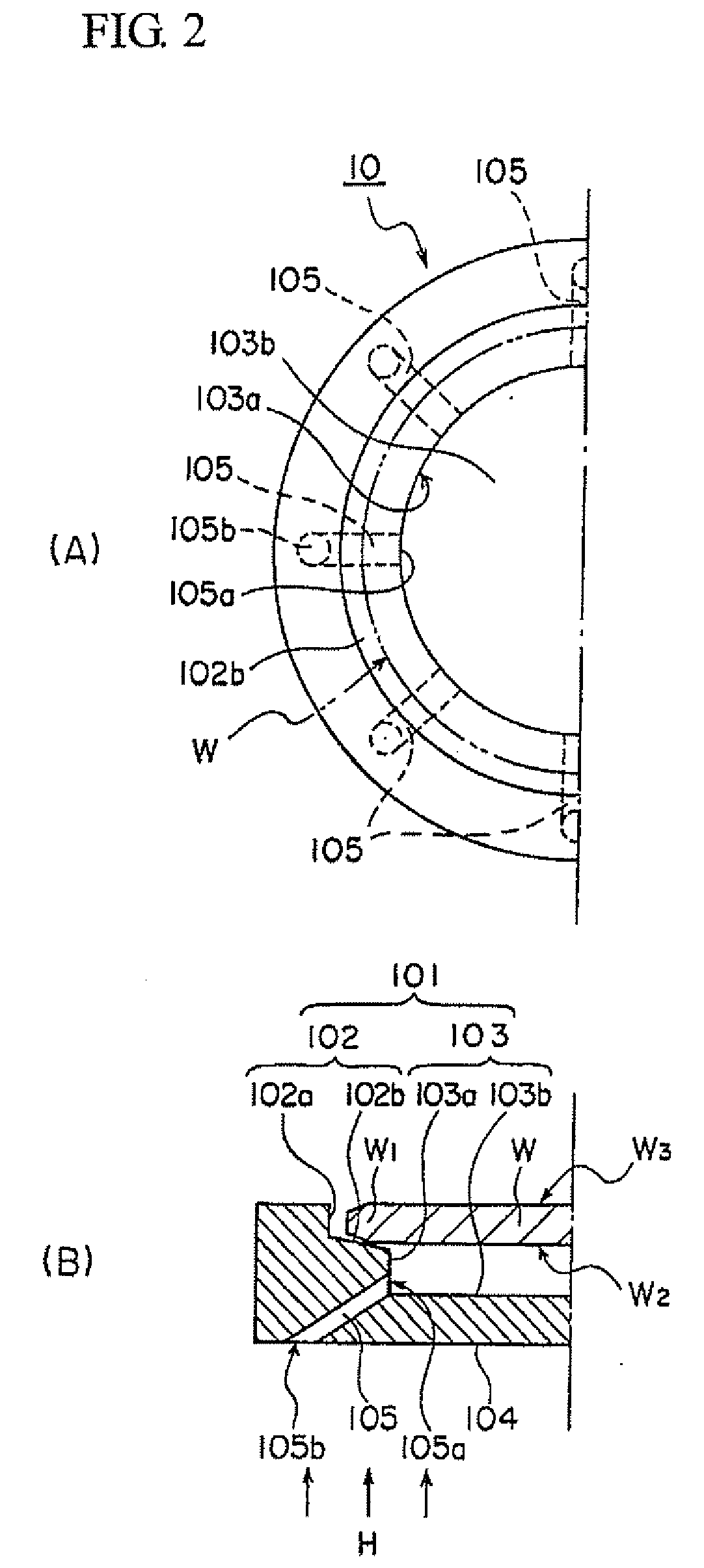
[0058]In the examples, the single wafer vapor-phase growth reactor shown in FIG. 1 was used and a susceptor having a shape shown in FIG. 3(C) was used. Specifically, holes composing a fluid passage (a large hole width was 2 mm, a small hole...


PUM

PropertyMeasurementUnit
depthaaaaaaaaaa
resistivityaaaaaaaaaa

Abstract

In a susceptor (10) having a wafer pocket (101) for receiving a wafer W at the time of vapor-phase growth, the wafer pocket has at least a first pocket portion (102) for loading an outer circumferential portion of the wafer and a second pocket portion (103) formed to be lower than the first pocket and having a smaller diameter than that of the first pocket portion, and a fluid passage (105) having one end (105a) opening on a vertical wall (103a) of said second pocket portion and the other end (105b) opening on a back surface (104) or a side surface (106) of the susceptor is formed.

Description

TECHNICAL FIELD[0001]The present invention relates to a susceptor used for a vapor-phase growth reactor for growing an epitaxial layer on a surface of a silicon wafer (hereinafter, simply referred to as a wafer) used for a semiconductor device and, particularly, relates to a susceptor for a vapor-phase growth reactor capable of suppressing rising of a dopant concentration of an outer circumferential portion of an epitaxial film caused by auto-doping.BACKGROUND ART[0002]As a vapor-phase growth reactor for growing an epitaxial film having a high quality film property on a wafer surface, a single wafer vapor-phase growth reactor is often used.[0003]This single wafer vapor-phase growth reactor grows an epitaxial film on a wafer surface by placing a wafer on a disk-shaped susceptor formed by coating silicon carbide SiC on graphite as a mother material in a channel-shaped chamber made by quartz and bringing the wafer react with various material gases passing through the chamber while heat...

Claims


Application Information

Patent Timeline
Patent Type & Authority Applications(United States)
IPC IPC(8): C23C16/02C23C16/458H01L21/205H01L21/68H01L21/687
CPCC23C16/4583H01L21/68785H01L21/68735C30B25/12C23C16/458H01L21/105H01L21/68
Inventor FUJIKAWA, TAKASHIISHIBASHI, MASAYUKIDOHI, TAKAYUKISUGIMOTO, SEIJI
Owner SUMCO CORP
Why Eureka
Try Eureka