Transfer substrate, transfer method, and method of manufacturing display device

a technology of transfer substrate and transfer method, which is applied in the direction of photosensitive materials, instruments, photomechanical equipment, etc., can solve the problems of deterioration in the production efficiency of the display device, and achieve the effect of effective formation of transfer patterns and improvement of production efficiency

Inactive Publication Date: 2008-05-15
JOLED INC
View PDF2 Cites 52 Cited by
  • Summary
  • Abstract
  • Description
  • Claims
  • Application Information

AI Technical Summary

Benefits of technology

[0010]Thus, it is desirable to provide a transfer substrate and a transfer method with which it is possible to effectively perform formation of transfer patterns by thermal transfer and realize improvement of production efficiency and a method of manufacturing a display device.
[0011]According to an embodiment of the invention, there is provided a transfer substrate including a transfer material layer on a support substrate via a light absorbing layer, wherein antireflection patterns for preventing light reflection on an interface of the support substrate and the light absorbing layer is provided between the support substrate and the light absorbing layer. Film thickness of this antireflection patterns is set to a value with which an absorptance of light having a predetermined wavelength absorbed in the light absorbing layer is maximized.

Problems solved by technology

This causes deterioration in production efficiency of the display device.

Method used


Image

  • Transfer substrate, transfer method, and method of manufacturing display device
  • Transfer substrate, transfer method, and method of manufacturing display device
  • Transfer substrate, transfer method, and method of manufacturing display device

Examples


first embodiment

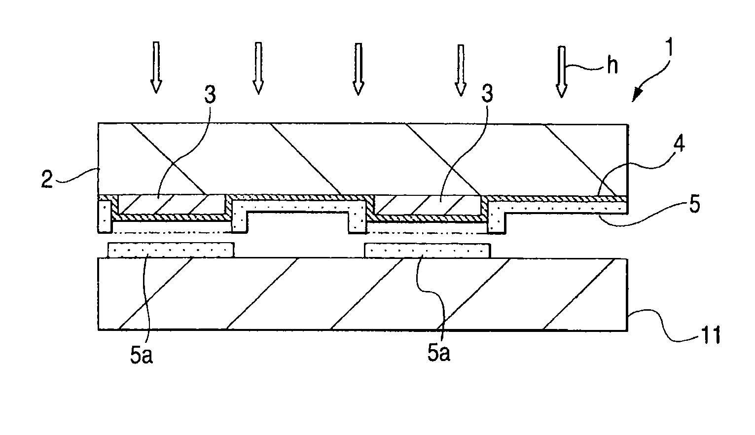
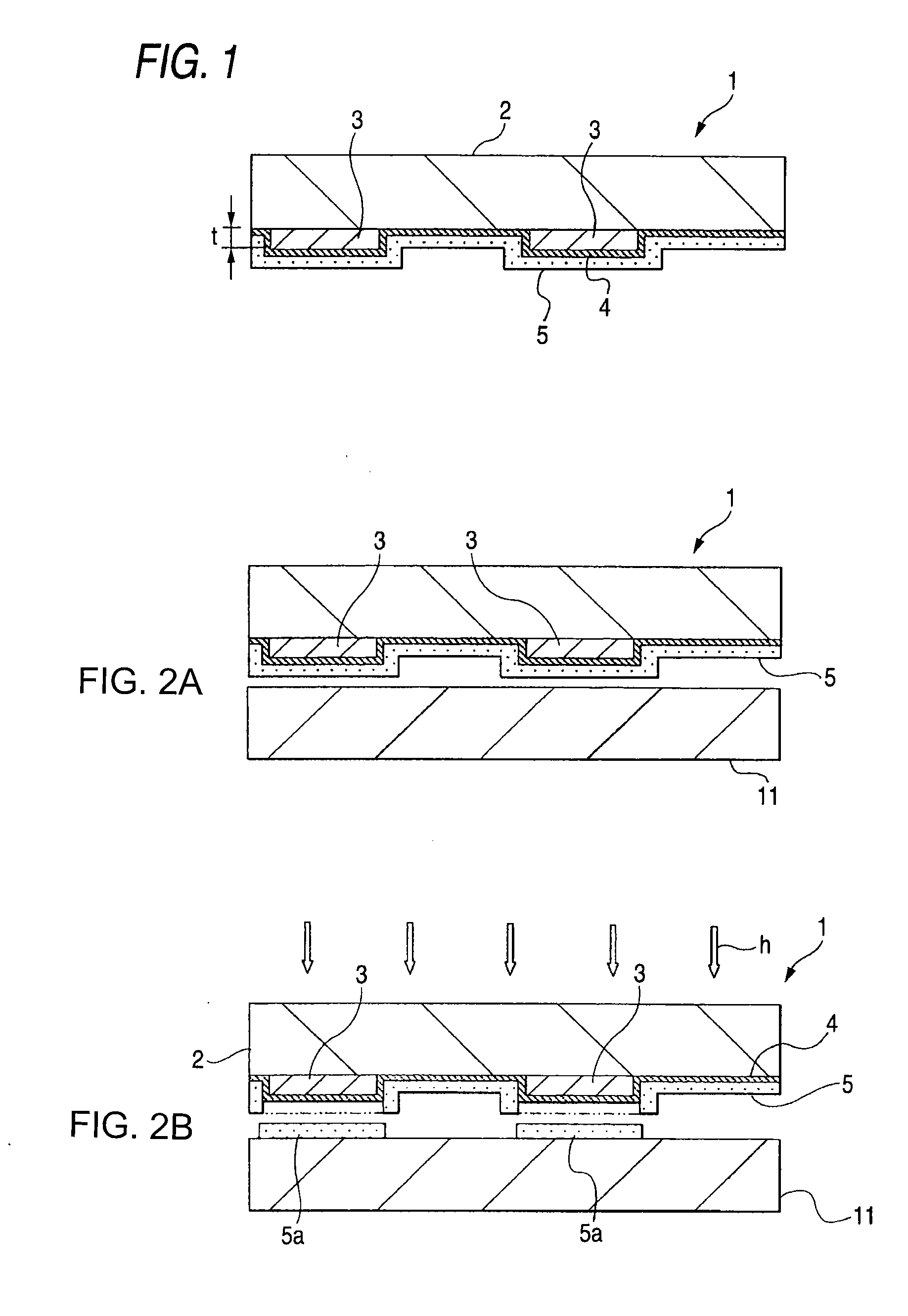
[0029]FIG. 1 is a main part sectional view for explaining a structure of a transfer substrate according to a first embodiment of the invention. A transfer substrate 1 shown in the figure includes a support substrate 2, antireflection patterns 3 provided on the support substrate 2, a light absorbing layer 4 provided on the support substrate 2 to cover the antireflection patterns 3, and a transfer material layer 5 provided on the light absorbing layer 4.

[0030]The support layer 2 has satisfactory light transmission properties with respect to light h having a predetermined wavelength irradiated in transfer in which the transfer substrate 1 is used. The support substrate 2 is made of, for example, a glass substrate.

[0031]The antireflection patterns 3 have an effect of preventing light reflection on an interface of the support substrate 2 and the light absorbing layer 4. As such antireflection patterns 3, in particular, antireflection patterns having a real part of a refractive index exce...

second embodiment

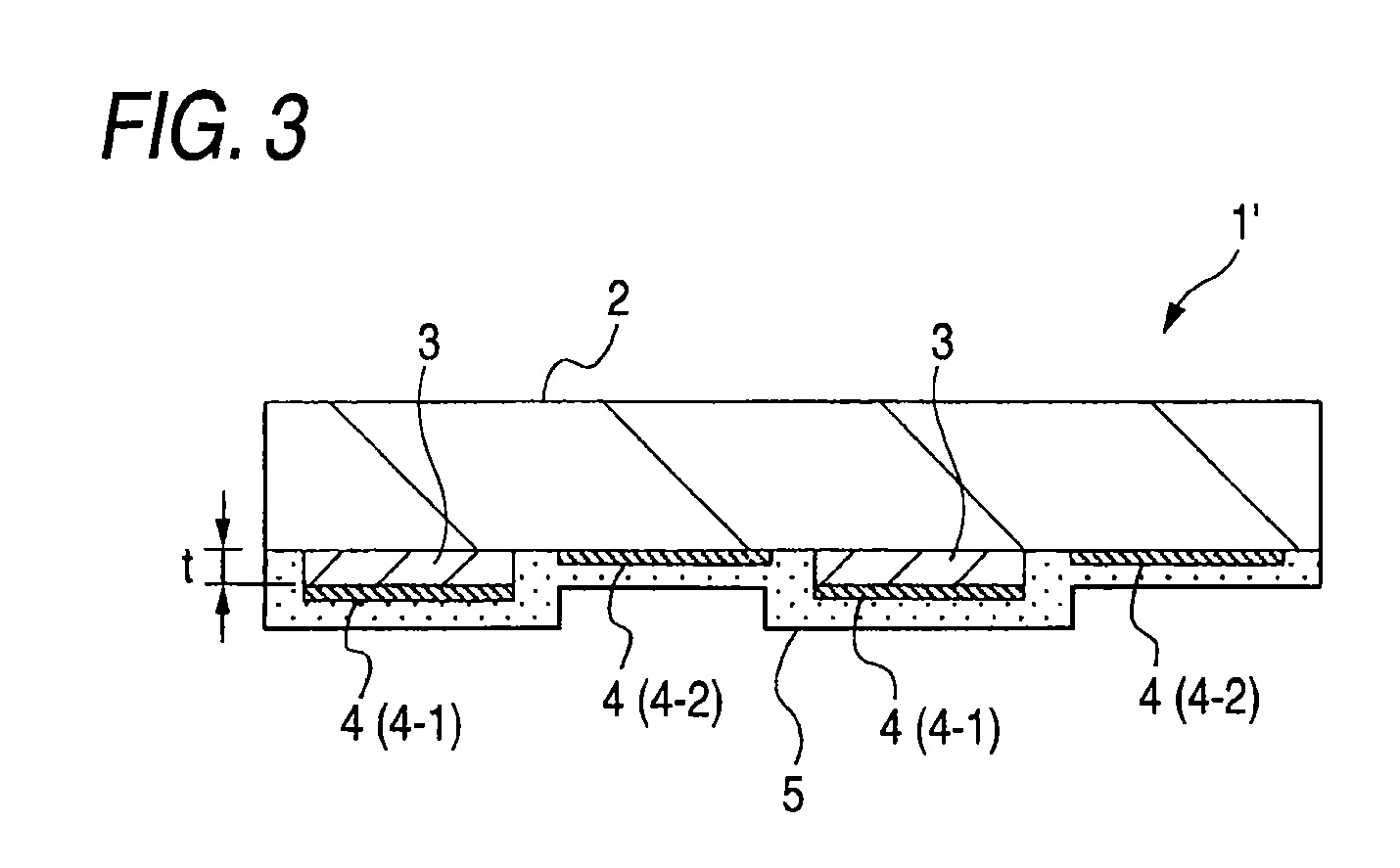
[0041]FIG. 3 is a main part sectional view for explaining a structure of a transfer substrate according to a second embodiment of the invention. A transfer substrate 1′ shown in the figure is different from the transfer substrate explained with reference to FIG. 1 in the first embodiment in that the light absorbing layer 4 is patterned, but otherwise the transfer substrate 1′ is the same as the transfer substrate.

[0042]The light absorbing layer 4 is patterned in portions where the antireflection patterns 3 are provided and portions where the antireflection patterns 3 are not provided. For example, in the portions where the antireflection patterns 3 are provided, the light absorbing layer 4 is patterned in a shape substantially identical with the antireflection patterns 3 and, in the portions where the antireflection patterns 3 are not provided, the light absorbing layer 4 is patterned in, for example, a shape identical with that on the antireflection patterns 3. An array state of li...

third embodiment

[0055]FIG. 5 is a main part sectional view for explaining a structure of a transfer substrate according to a third embodiment of the invention. A transfer substrate 1″ shown in the figure is suitably used in manufacturing a full color display device in which an organic electroluminescence element is used. Components identical with those in the first and the second embodiments are denoted by the identical reference numerals and signs and redundant explanations are omitted.

[0056]The transfer substrate 1″ shown in the figure includes the support substrate 2, antireflection patterns 3-1, 3-2, and 3-3 provided on the support substrate 2, the light absorbing layers 4 formed on the antireflection patterns 3-1, 3-2, and 3-3, and the transfer material layer 5 provided on the light absorbing layers 4.

[0057]The support substrate 2 has satisfactory light transmission properties with respect to lights h1 to h3 having predetermined wavelengths irradiated in transfer in which the transfer substrat...


PUM

PropertyMeasurementUnit
refractive indexaaaaaaaaaa
thicknessaaaaaaaaaa

Abstract

A transfer substrate includes a transfer material layer on a support substrate via a light absorbing layer. Antireflection patterns for preventing light reflection on an interface of the support substrate and the light absorbing layer are provided between the support substrate and the light absorbing layer. Thickness of this antireflection patterns is set to a value with which an absorptance of light having a predetermined wavelength absorbed in the light absorbing layer is maximized.

Description

CROSS-REFERENCES TO RELATED APPLICATIONS[0001]The present invention contains subject matter related to Japanese Patent Application JP 2005-335310 filed in the Japanese Patent Office on Nov. 21, 2005, the entire contents of which being incorporated herein by reference.BACKGROUND OF THE INVENTION[0002]1. Field of the Invention[0003]The present invention relates to a transfer substrate and a transfer method for sublimating, with irradiation of a heat source, a transfer material layer formed on a support substrate and transferring the transfer material layer to a receptor substrate side and a method of manufacturing a display device to which this transfer method is applied.[0004]2. Description of the Related Art[0005]An organic electroluminescence element that utilizes electroluminescence of an organic material includes an organic layer, in which a hole transport layer and a light emitting layer are stacked, between a lower electrode and an upper electrode. The organic electroluminescen...

Claims


Application Information

Patent Timeline
Patent Type & Authority Applications(United States)
IPC IPC(8): G03F7/004
CPCH01L27/3211H01L51/0013H01L2251/558H01L51/5284H01L51/0059H10K59/35H10K71/18H10K85/631H10K50/865H10K2102/351H05B33/10H05B33/14
Inventor MATSUO, KEISUKE
Owner JOLED INC
Why Eureka
Try Eureka